Intel® 460GX Chipset Software Developer’s Manual 12-5
IDE Configuration
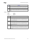
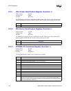
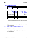
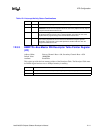
12.2.8 SVID–Subsystem Vendor ID (Function 1)
Address: 2C-2Dh
Default Value: 0000h
Attribute: Read only
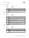
12.2.9 SID–Subsystem ID (Function 1)
Address: 2E-2Fh
Default Value: 0000h
Attribute: Read only
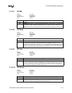
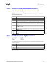
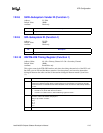
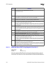
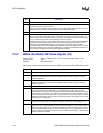
12.2.10 IDETIM–IDE Timing Register (Function 1)
Address Offset: 40–41h = Primary Channel 42–43h = Secondary Channel
Default Value: 0000h
Attribute: Read/Write only
This register controls the IFB's IDE interface and selects the timing characteristics of the PCI Local
Bus IDE cycle for PIO and Bus Master transfers. Note that primary and secondary denotations
distinguish between the cables and the 0/1 denotations distinguish between master (0) and slave
(1).
Bit Description
15:0 Subsystem Vendor ID.
Bit Description
15:0 Subsystem ID.
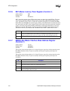
Bit Description
15 IDE Decode Enable (IDE). 1=Enable. 0=Disable. When enabled, I/O transactions on PCI
targeting the IDE ATA register blocks (command block and control block) are positively decoded
on PCI and driven on the IDE interface. When disabled, these accesses are subtractively decoded
to LPC.
14 Slave IDE Timing Register Enable (SITRE).
0 Use bits 13:12, 9:8 for both drive 0 and drive 1.
1 Use bits 13:12, 9:8 for drive 0, Slave IDE timing register for drive 1.
13:12 IORDY Sample Point (ISP). This field selects the number of PCI clocks between IOR#/IOW#
assertion and the first IORDY sample point.
Bits[13:12] Number of Clocks
00 5
01 4
10 3
11 2
11:10 Reserved.


