


IDE Configuration
12-8 Intel® 460GX Chipset Software Developer’s Manual
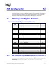
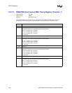
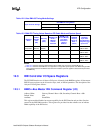
12.2.13 SDMATIM–Synchronous DMA Timing Register (Function 1)
Address Offset: 4A-4Bh
Default Value: 0000h
Attribute: Read/Write only
This register controls the timings used by each Synchronous DMA enabled device. For non-
synchronous DMA operation, this register should be left programmed to its default value.
Bit Description
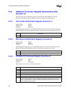
15:14 Reserved.
13:12 Secondary Drive 1 Cycle Time (SCT1): These bit settings determine the minimum data write
strobe Cycle Time (CT) and minimum Ready to Pause time (RP).
00: CT = 4 PCICLK, RP = 6 PCICLK
01: CT = 3 PCICLK, RP = 5 PCICLK
10: CT = 2 PCICLK, RP = 4 PCICLK
11: Reserved
11:10 Reserved.
9:8 Secondary Drive 0 Cycle Time (SCT0): These bit settings determine the minimum data write
strobe Cycle Time (CT) and minimum Ready to Pause time (RP).
00: CT = 4 PCICLK, RP = 6 PCICLK
01: CT = 3 PCICLK, RP = 5 PCICLK
10: CT = 2 PCICLK, RP = 4 PCICLK
11: Reserved
7:6 Reserved.
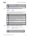
5:4 Primary Drive 1 Cycle Time (PCT1): These bit settings determine the minimum data write
strobe Cycle Time (CT) and minimum Ready to Pause time (RP).
00: CT = 4 PCICLK, RP = 6 PCICLK
01: CT = 3 PCICLK, RP = 5 PCICLK
10: CT = 2 PCICLK, RP = 4 PCICLK
11: Reserved
3:2 Reserved.
1:0 Primary Drive 0 Cycle Time (PCT0): These bit settings determine the minimum data write
strobe Cycle Time (CT) and minimum Ready to Pause time (RP).
00: CT = 4 PCICLK, RP = 6 PCICLK
01: CT = 3 PCICLK, RP = 5 PCICLK
10: CT = 2 PCICLK, RP = 4 PCICLK
11: Reserved