Register Descriptions
2-4 Intel® 460GX Chipset Software Developer’s Manual
2.2.6 Consistency
There are a number of registers that are repeated in both the SAC and xXB/PCI spaces. It is
software’s responsibility to insure that these registers are programmed in a consistent fashion.
Failure to insure consistency can produce indeterminate results. See the Initialization Chapter for
an overview on initializing all chipset components.
When the address decode ranges of 460GX chipset devices are being updated, no other bus traffic
is allowed over the address ranges being affected by the update. This means that the code that
updates initial configuration must be executing from a location that will not be affected by the
update. Furthermore in a multiprocessor system, precautions should be taken to assure that only
one CPU is accessing configuration space at a time.
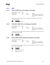
2.2.7 GART Programming Region
The region starting at FE20_0000h is used for programming the GARTs. This region is accessible
either by the processor or PCI. See Section 7.2.1 for GART programming details
2.3 I/O Mapped Registers
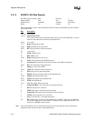
The 460GX chipset contains two registers that reside in the CPU I/O address space: the
Configuration Address (CONFIG_ADDRESS) Register and the Configuration Data
(CONFIG_DATA) Register. The Configuration Address Register enables/disables the
configuration space and determines what portion of configuration space is visible through the
Configuration Data window. The following sections define the fields within the
CONFIG_ADDRESS and CONFIG_DATA registers. The 460GX chipset’s device ID mapping
into the CONFIG_ADDRESS definition is shown in Table 2-1.
2.3.1 CONFIG_ADDRESS: Configuration Address Register
I/O Address: CF8h [Dword] Size: 32 bits
Default Value: 00000000h Attribute: Read/Write
Sticky: No Locked: No
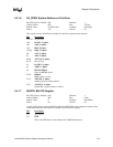
CONFIG_ADDRESS is a 32 bit register accessed only when referenced as a Dword. A Byte or
Word reference will “pass through” the Configuration Address Register onto the PCI bus as an I/O
cycle. The CONFIG_ADDRESS register contains the Bus Number, Device Number, Function
Number, and Register Number for which a subsequent configuration access is intended.
Bits
Description
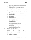
31 Configuration Enable(CFGE).
When this bit is set to 1 accesses to PCI configuration space are enabled. If this bit is reset
to 0 accesses to PCI configuration space are disabled.
30:24 reserved (0)
23:16 Bus Number.
When the Bus Number is programmed to match the Chipset Bus Number (CBN), the
target of the Configuration Cycle is the 460GX chipset. If the Bus Number is not CBN,
the destination and type of access is determined by the Bus Number and Subordinate Bus
Number of each PCI port in each PXB. A type 0 access is generated on the appropriate
PCI bus if one of the PXB port’s bus number is matched. Otherwise, a type 1
configuration cycle is generated on the appropriate PCI bus below the PXB port whose


