Memory Subsystem
5-4 Intel® 460GX Chipset Software Developer’s Manual
5.2 Interleaving/Configurations
Maximum system bandwidth is obtainable in several ways. If the address patterns are well-behaved
then one can use the page mode of the DRAM itself to obtain high bandwidths. Generally page hits
can sustain about 5 times the bandwidth of page misses with a one-bank memory system. In
systems with only several memory banks, designs tend to try and optimize the page hit rate to
increase bandwidth.
A second approach is to have as many parallel operations within the memory system as possible.
One can spread the addresses out across multiple DRAMs and have the data transfers in parallel.
This lends itself well to designs which require a large memory system of many gigabytes.
The 460GX will implement the second approach. It will attempt to increase the amount of
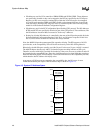
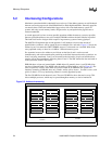
parallelization. Addresses will be spread out across multiple rows and cards. Figure 5-2 shows the
address layout. It assumes that 2Mx72 DIMMs are used, so that each row is 64 MB. With all the
rows populated evenly we have 16 x 64 MB or 1 GB total memory space.
For sequential accesses, the addresses are laid out so that lines 0 and 1 can be accessed
simultaneously, and can be transferred in parallel up to the final data transfer on the system bus. As
0 and 1 are being transferred, 2 and 3 can be started to the left stacks of each card and their data
transfer will be done immediately following that of 0 and 1. The SDC buffers the data and sends it
to the system bus with no dead cycles.
SDRAMs have at least two internal banks; 64Mb chips will generally have 4, and 256 Mb chips
may have 8 internal banks. The 460GX takes advantage of these banks as well. In Figure 5-2, the
rows are split into 2 halves. Since there are at least 2 banks in all SDRAMs, the system will
interleave assuming all DRAMs have only 2 banks, and be split as shown. So with 16 rows, each
split in 2, there is a 32 way interleaving scheme in a totally populated system.
The first 256 MB lies in the bottom 4 rows. The next 256 MB lies above that and so on up. This
allows multiple processes, which may be spread throughout memory, to also be interleaved.
Figure 5-2. Address Interleaving
Card A
Card B
Line 2,10,...
Line 6,14,...
256M+2,256M+10,...
256M+6,256M+14,...
512M+2,512M+10,...
512M+6,512M+14,...
768M+2,768M+10,...
768M+6,768M+14,...
Line 1,9,...
Line 5,13,...
256M+1, 256M+9,...
256M+5, 256M+13,...
512M+1,512M+9,...
512M+5,512M+13,...
768M+1,768M+9,...
768M+5,768M+13,...
Line 3,11,...
Line 7,15,...
256M+3,256M+11,...
256M+7,256M+15,...
512M+3,512M+11,...
512M+7,512M+15,...
768M+3,768M+11,...
768M+7,768M+15,...
Line 0,8,...
Line 4,12,...
256M,256M+8,...
256M+4, 256M+12,...
512M,512M+8,...
512M+4,512M+12,...
768M,768M+8,...
768M+4,768M+12,...


