Intel® 460GX Chipset Software Developer’s Manual 11-35
LPC/FWH Interface Configuration
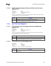
11.2.7.7 General Purpose 1 Status
Address Offset: 16-17h
Attributes: Read/Write
Default Value: 0000h
Size: 16 bits
When any bit is set in this register, and the corresponding bit is enabled in the General Purpose 1
Enable register, an SCI and a wake event will be generated.
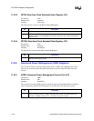
11.2.7.8 General Purpose 1 Enable
Address Offset: 18-19h
Attributes: Read/Write
Default Value: 0000h
Size: 16 bits
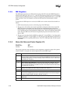
11.2.8 SMI Registers
In addition to the ACPI I/O registers, there are some generic registers that are defined for legacy
based SMI# logic. These I/O registers are added to the end of the I/O register space defined by the
ACPI block. All reserved bits will always return 0 when read, and will have no effect when written.
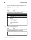
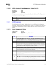
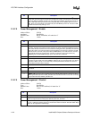
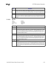
1 NMI_EN: This bit enables an SCI to be generated on a NMI event. Upon power up, this bit is set
to ‘0’.
0 THRM_EN: This is the thermal enable bit. When this bit is set an active level assertion of the
THRM# signal (as defined by the THRM_POL bit) will set the THRM_STS bit and generate a
power management event (an SCI or SMI). Upon power up, this bit is set to ‘0’.
Bit Description
Bit Description
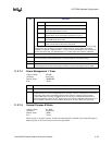
15:9 Reserved.
8:0 GPIO_STS: Each bit corresponds to a single GPIO bit (Ex: Bit 8 refers to GPIO[8]. This bit is set
when the data bit in the GPIO data register is set to a ‘1’, and cleared by software writing a ‘1’ to
this bit location. Additionally, if the GPIO_EN bit in the General Purpose 1 Enable Register is
set, then the setting of this bit will generate an SCI or wake event.
Bit Description
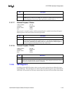
15:9 Reserved.
8:0 GPIO_EN: Each bit corresponds to a single GPIO bit (Ex: Bit 8 refers to GPIO8). When set, the
setting of the corresponding bit in the General Purpose 1 Status Register will generate an SCI or
wake event. These bits are not cleared on a CF9 reset.


