System Address Map
4-4 Intel® 460GX Chipset Software Developer’s Manual
— FEB0_0CC0: This address is used for BSP selection. It is a write once register in the
SAC.
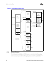
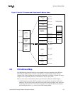
Figure 4-1 shows how the SAPIC and GART spaces are allocated. There may be up to 255 I/O
SAPICs in the system. There is one region defined for the GART space.
4.1.3.1 Variable GAP
The variable gap starts at 4G-32M, and can grow downward in 32M increments. This gap is used to
provide memory mapped I/O spaces to all of the logical PCI buses (this includes AGP buses) in the
system. Each logical PCI bus is allowed n x 32M of contiguous space. PCI bus #0 is allowed the
first a*32M below (4G-32M), PCI bus #1 is allowed the next b*32M, PCI bus #2 is allowed the
next c*32M, etc. The total gap size, n, is equal to a + b + c and so on. The combined size of the
variable and the fixed gaps must equal a multiple of 64 MB. Since the variable gap starts on a
32 MB boundary, the variable gap must total to an odd multiple of 32 MB. This limit is set up by
firmware and is a function of the memory controller design.
4.1.4 High Extended Memory (above 4G)
The entire address space above 4 GB is treated by the 460GX chipset as ordinary memory. The top
of system memory is calculated by firmware. Processor accesses above the top of system memory
are still claimed by the chipset, but are not forwarded to memory or PCI; instead they cause a
BINIT#. Inbound accesses to this region can only occur due to a programming or address parity
error. Firmware programs both the PXBs and GXBs with the Top of Memory value. A
programming error that results in a PXB access above the Top of Memory causes the PXB to route
the request as if it were to a peer PCI bus. Therefore the request goes through the SAC decoder and
causes a BINIT#. A programming error that results in a GXB access above the Top of Memory
(detected after GART translation) causes the GXB to force a BINIT#. Address parity errors are
detected at each of the major bus interfaces.
4.1.5 Re-mapped Memory Areas
Any DRAM that lies behind an address that is mapped to PCI or is reserved in the region below
4 GB and above 1 MB is recovered. The memory that lies in the Medium Extended Memory
Region is moved so that it is addressed above 4 GB. This covers all addresses in the Medium
Extended Memory Region. For example, if there is 3 GB of memory and the Medium Extended
Memory Region is 2 GB total (covering PCI, AGP and the reserved area), then the first 2 GB of
addresses are directed to DRAM, the next 2 GB of addresses are directed to PCI or are AGP
addresses or reserved, and the address range between 4 GB and 5 GB would be directed to DRAM.
In other words, to access the 2 GB+1 byte of memory, the processor would use address 4 GB+1,
since the physical address of 2 GB+1 is now mapped to PCI.
Any DRAM not used in the Low Extended Memory Region, i.e. the region below 1 MB is not
recovered. The DRAM in this region which has its address directed to PCI is simply lost to the
system.


