Intel® 460GX Chipset Software Developer’s Manual 9-1
IFB Register Mapping 9
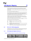
The IFB internal registers are organized into four Functions–LPC/FWH interface bridge, IDE
Controller, USB Host Controller, and Enhanced Power Management. Each Function has its
registers divided into 1 set of PCI Configuration Registers and one or more register sets located in
system I/O space.
Software should not map programmable memory or I/O address registers such that any part of the
range overlaps addresses decoded by other IFB devices.
Some of the IFB registers contain reserved bits. Software must deal correctly with fields that are
reserved. On reads, software must use appropriate masks to extract the defined bits and not rely on
reserved bits being any particular value. On writes, software must ensure that the values of
reserved bit positions are preserved. That is, the values of reserved bit positions must first be read,
merged with the new values for other bit positions and then written back.
In addition to reserved bits within a register, the IFB contains address locations in the PCI
configuration space that are marked “Reserved”. The IFB responds to accesses to these address
locations by completing the Host cycle. Software should not write to reserved IFB configuration
locations in the device-specific region (above address offset 3Fh).
During a hard reset, the IFB sets its internal registers to predetermined default states. The default
values are indicated in the individual register descriptions.
The following notation is used to describe register access attributes:
RO Read Only. If a register is read only, writes have no effect.
WO Write Only. If a register is write only, reads have no effect.
R/W Read/Write. A register with this attribute can be read and written. Note that individual
bits in some read/write registers may be read only.
R/WC Read/Write Clear. A register bit with this attribute can be read and written. However, a
write of a 1 clears (sets to 0) the corresponding bit and a write of a 0 has no effect.
9.1 PCI / LPC / FWH Configuration
The IFB PCI Function 0 contains a LPC/FWH interface, interrupt controller and counter / timers,
including the real time clock. The register set associated with this Functionality and associated
logic is shown below with actual register descriptions given in this section.
9.1.1 PCI Configuration Registers (Function 0)
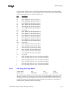
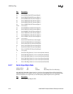
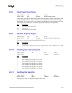
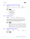
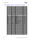
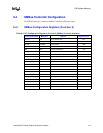
Table 9-1. PCI Configuration Registers–Function 0(PCI to LPC/FWH Interface Bridge)
Configuration Offset Mnemonic Register Register Access
00–01h VID Vendor Identification RO
02–03h DID Device Identification RO
04–05h PCICMD PCI Command R/W


