Memory Subsystem
5-6 Intel® 460GX Chipset Software Developer’s Manual
5.4 Memory Subsystem Clocking
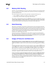
The DIMMs are clocked at half the system bus frequency. For the Itanium processor, this means
the DRAMs are clocked at 15 ns. Data is clocked out at the rate of 32B per 15 ns.
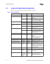
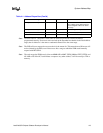
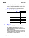
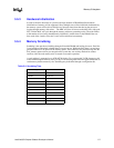
The following table lists the DRAM parameters used for the 460GX chipset.
5.5 Supporting Features
5.5.1 Auto Detection
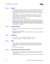
The memory controller provides capability for auto-detection of SDRAM type installed in the
system during the system configuration and initialization, providing a Plug-and-Play DRAM
interface to the user. This is done through the Serial Presence Detect logic on the DIMM. Firmware
will read the Serial Presence Detect (SPD) for each row to determine the size of the memory in that
row. Firmware will then write the size and interleaving information into the SAC and MAC
through configuration cycles. Firmware will not have to go write data and see if it is there and do
any addressing schemes to understand the system configuration. It will simply read a configuration
register and then write a different configuration register with the chipset mapping. At the same time
Firmware can calculate total system memory.
5.5.2 Removing a Bad Row
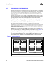
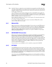
A row of memory may have a chip or DIMM fail. If an un-correctable error occurs, the system will
machine-check, usually resulting in a reset. The 460GX will report which row failed. During the
next re-boot or at power on, if the memory test fails, firmware may map the failing row as if it
didn’t exist. Since firmware goes through and reads the SPD on each row to determine its size,
firmware can just set that particular row to a size of 0, as if it weren’t there. No addresses will then
be sent to that row. The entire row is removed, even if only one side of a double-sided DIMM were
bad. But only the failing row is disabled. All other rows are still present, and the interleaving
scheme will make the maximum use of the remaining rows. For example, a system with 8 rows
populated that has one go bad will be restarted with 7 rows available.
Table 5-3. Required DRAM Parameters
Parameter Symbol
Min.
(clocks)
Max.
(clocks)
Clock cycle time at CL=2 Tck 15 ns.
Access time from CLK Tac 6 ns.
CAS Latency TCL 2
RAS latency 4
RAS cycle time Trc 6
RAS to CAS delay Trcd 2
RAS precharge Trp 2
Data to precharge Tdpl
a
a. The sum of Tdpl and Trp are equal to Tdal as defined in the PC SDRAM Specification.
1


