Intel® 460GX Chipset Software Developer’s Manual 2-9
Register Descriptions
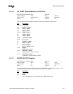
2.4.1.6 SA_FERR: System Address on First Error
Bus CBN, Device Number: 00h Function: 1
Address Offset: 60h Size: 128 bits
Default Value: undefined after Attribute: Read Only
Sticky: Yes Locked: No
This register records and latches the address for the first system bus error detected.
Bits
Description
127:107 Reserved (0)
106 LOCK, ’b’ phase.
105 ADS, ’b’ phase.
104 RP#, ’b’ phase.
103:99 REQ, ’b’ phase.
98 AP1; ’b’ phase.
97 AP0; ’b’ phase.
96:64 A[35:3]#, ’b’ phase.
63:43 Reserved (0)
42 LOCK#, ’a’ phase.
41 ADS#, ’a’ phase.
40 RP# for REQa#.
Parity on REQa# signals.
39:35 REQa#.
REQa signals on error.
34:33 AP[1:0]#, ’a’ phase.
Address parity for failing address.
32:0 Aa[35:3]#, ’a’ phase.
System Bus - System Address of Error.
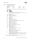
2.4.1.7 BIUITID: BIU ITID Register
Bus CBN, Device Number: 00h Function: 1
Address Offset: 80h Size: 8 bits
Default Value: 0 Attribute: Read/Write
Sticky: No Locked: No
A write to this register causes the SAC to update the BIUDATA register with the contents of the
CAM and RAM associated with the ITID that is written into this register.
Bits
Description
7:6 reserved (0)
5:0 ITID
This is the ITID that is used to address the CAM/RAM structure.


