Register Descriptions
2-14 Intel® 460GX Chipset Software Developer’s Manual
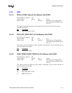
2.4.2.11 DED1_ECC_FERR: ECC on First Memory Card A DED
Bus CBN, Device Number: 04h
Address Offset: 78h Size: 8 bits
Default Value: 00h Attribute: Read Only, New Value Latched
anytime appropriate FERR register
bit is set
This register records and latches the ECC checkbits corresponding to the first DED detected by
memory interface 0 in the SDC.
Bits
Description
7:0 ECC - ECC of Error.
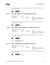
2.4.2.12 DED1_TXINFO_FERR: TXINFO on First Memory Card A DED
Bus CBN, Device Number: 04h
Address Offset: 79-7Ah Size: 16 bits
Default Value: 00h Attribute: Read Only, New Value Latched
anytime appropriate FERR register
bit is set
This register records the ITID and failing chunk corresponding to the first DED detected by
memory interface 1 in the SDC.
Bits
Description
15:9 reserved(0)
8:6 DC - Data Chunk of ITID.
5:0 ITID - ITID of error.
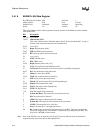
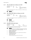
2.4.2.13 SDC_FERR: First Error Status Register
Bus CBN, Device Number: 04h
Address Offset: 80-83h Size: 32 bits
Default Value: 0000h Attribute: Read/Write to Clear
This register records the first error condition detected in the SDC. Writing a ’1’ to this register will
clear the bit in both SDC_FERR and the same bit in SDC_NERR.
Bits
Description
31 Simultaneous S/W write-one-to-clear and H/W error detected in the same cycle. This bit
will only be set if another bit is also set. This implies that the ERROR>_<TYPE>_FERR
data registers associated with the other asserted bit contain stale data.
30 PDB Receive Length Error (RLE)
Private Bus receive length error
29 DRDY# Protocol Error (FS2)
Asserted when a protocol error is found involving DRDY#, SBUSY# and DBUSY#.
28 Write Data Protocol Error (FS1)
Asserted on write protocol errors.
27 LEN# Protocol Error (FS0)
Asserted on mismatches of LEN# field and actual data transmitted.


