Intel® 460GX Chipset Software Developer’s Manual 15-17
PCI/LPC Bridge Description
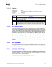
15.5.1.4 Register D
Address Offset: 0Dh
Default Value: NA - This register is not affected by any system reset signal.
Attribute: Read/Write
This register is used for various flags.
15.5.2 RTC Update Cycle
An update cycle occurs once a second, if the SET bit of register B is not asserted and the divide
chain is properly configured. During this procedure, the stored time and date will be incremented,
overflow will be checked, a matching alarm condition will be checked, and the time and date will
be rewritten to the RAM locations. The update cycle will start at least 244µs after the UIP bit of
register A is asserted, and the entire cycle will not take more than 1984µs to complete. The time
and date RAM locations (0-9) will be disconnected from the external bus during this time. To avoid
update and data conditions, external RAM access to these locations can safely occur at two times.
When a updated-ended interrupt is detected, almost 999ms are available to read and write valid
time and date data. If the UIP bit of register A is detected to be low, there is at least 244µs before
the update cycle begins. Because the overflow conditions for leap years and daylight savings
adjustments are based on more than one date or time item, the time before one of these conditions
should be set (when adjusting) at least two seconds before one of these conditions to ensure proper
operation.
15.5.3 RTC Interrupts
The real-time clock interrupt is internally routed within the IFB both to the I/O APIC and the 8259.
It is mapped to interrupt vector 8. This interrupt is not shared with any other interrupt. IRQ8# from
the serial stream is ignored.
15.5.4 Lockable RAM Ranges
The real-time clock battery-backed RAM supports two 8-byte ranges that can be enabled via the
configuration space. If the configuration bits are set, the corresponding range in the RAM will not
be readable or writeable. A write cycle to those locations will have no effect. A read cycle to those
locations will not return the actual location value.
Once enabled, this Function can only be disabled by a hard reset.
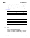
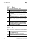
Bit(s) Description
7 Valid RAM and TIME Bit (VRT): The Valid Ram and Time bit is set to one when the PWRGD
(power good) signal provided is high. This feature is not typically used. This bit should always be
set to 0 for write to this register.
6 Reserved. This bit always returns a 0 and should be set to 0 for write cycles.
5:0 Date Alarm (DA): These bits store the date of month alarm value. If set to 000000, then a don’t
care state is assumed. The host must configure the date alarm for these bits to do anything, yet
they can be written at any time. If the date alarm is not enabled, these bits will return zeros to
mimic the Functionality of the Motorola 146818B. These bits are not affected by RSMRST#.


