Intel® 460GX Chipset Software Developer’s Manual 12-1
IDE Configuration 12
The IFB PCI Function 1 contains an IDE Controller capable of Programmed I/O (PIO) transfers as
well as Bus Master transfer capability. It also supports the “Ultra DMA/33” synchronous DMA
mode of data transfer. The register set associated with IDE Controller is shown below.
12.1 PCI Configuration Registers (Function 1)
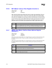
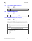
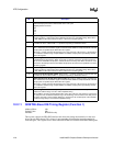
12.2 IDE Controller Register Descriptions (PCI Function 1)
This section describes in detail the registers associated with the IFB IDE Controller Function. This
includes Programmed I/O (PIO), Bus Master, and “Ultra DMA/33” synchronous DMA
Functionality.
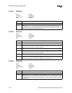
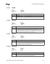
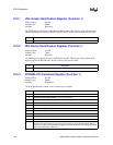
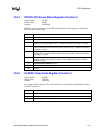
Table 12-1. PCI Configuration Registers–Function 1 (IDE Interface)
Configuration
Offset
Mnemonic Register Register Access
00–01h VID Vendor Identification RO
02–03h DID Device Identification RO
04–05h PCICMD PCI Command R/W
06–07h PCISTS PCI Device Status R/W
08h RID Revision Identification RO
09-0Bh CLASSC Class Code RO
0Ch – Reserved –
0Dh MLT Master Latency Timer R/W
0Eh HEDT Header Type RO
0F–1Fh – Reserved –
20–23h BMIBA Bus Master Interface Base Address R/W
24–3Bh – Reserved –
2C–2Dh SVID Subsystem Vendor ID RO
2E–2Fh SID Subsystem ID RO
30–3Fh – Reserved –
40–43h IDETIM IDE Timing R/W
44h SIDETIM Slave IDE Timing R/W
45–47h – Reserved –
48h SDMACTL Synchronous DMA Control R/W
49h – Reserved –
4A–4Bh SDMATIM Synchronous DMA Timing R/W
4C–FFh – Reserved –


