Intel® 460GX Chipset Software Developer’s Manual 11-29
LPC/FWH Interface Configuration
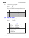
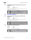
11.2.4.2 NmiEN–Nmi Enable Register (Shared with Real-time Clock Index
Register) (I/O)
I/O Address: 070h
Default Value: Bit[6:0]=undefined; Bit 7=1
Attribute: Write Only
This port is shared with the real-time clock. Do not modify the contents of this register without
considering the effects on the state of the other bits.
11.2.5 Real Time Clock Registers
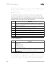
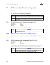
11.2.5.1 RTCI–Real-time Clock Index Register (Shared with NMI Enable
Register) (I/O)
I/O Address: 070h
Default Value: Bit[6:0]=Undefined; Bit 7=1
Attribute: Write Only
This port is shared with the NMI enable. Do not modify the contents of this register without
considering the effects on the state of the other bits.
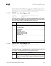
11.2.5.2 RTCD–Real-time Clock Data Register (I/O)
I/O Address: 071h
Default Value: Undefined
Attribute: Read/Write
The data port for accesses to the RTC standard RAM bank.
Bit Description
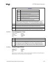
7 NMI Enable. 1=Disable generation of NMI; 0=Enable generation of NMI.
6:0 Real Time Clock Address. Used by the Real Time Clock to address memory locations. Not
used for NMI enabling/disabling. See description in Section 11.2.5.1.
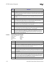
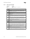
Bit Description
7 NMI Enable. Used by IFB NMI logic.
6:0 Real Time Clock Address. Latched by the Real Time Clock to address memory locations
within the standard RAM bank accessed via the Real Time Clock Data Register (071h).
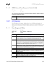
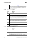
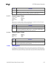
Bit Description
7:0 Standard RAM Data Port. Data written to standard RAM bank address selected via RTC Index
Register (070h).


