


LPC/FWH Interface Configuration
11-30 Intel® 460GX Chipset Software Developer’s Manual
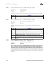
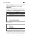
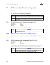
11.2.5.3 RTCEI–Real-time Clock Extended Index Register (I/O)
I/O Address: 072h
Default Value: Unknown
Attribute: Write Only
The index port for accesses to the RTC extended RAM bank.
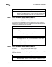
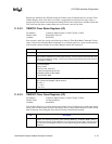
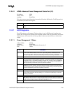
11.2.5.4 RTCED–Real-time Clock Extended Data Register (I/O)
I/O Address: 073h
Default Value: Unknown
Attribute: Read/Write
The data port for accesses to the RTC extended RAM bank.
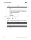
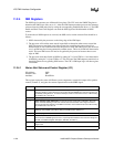
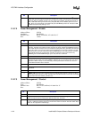
11.2.6 Advanced Power Management (APM) Registers
This section describes two power management registers–APMC and APMS Registers. These
registers are located in normal I/O space and must be accessed (via the PCI Bus) with 8 bit
accesses.
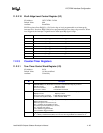
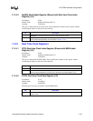
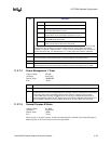
11.2.6.1 APMC–Advanced Power Management Control Port (I/O)
I/O Address: 0B2h
Default Value: 00h
Attribute: Read/Write
This register passes data (APM Commands) between the OS and the SMI handler. In addition,
writes can generate an SMI. The IFB operation is not effected by the data in this register.
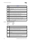
Bit Description
7 Reserved.
6:0 Real Time Clock Extended Address. Latched by the Real Time Clock to address memory
locations within the extended RAM bank accessed via the Real Time Clock Extended Data
Register (073h).
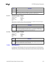
Bit Description
7:0 Extended RAM Data Port. Data written to standard RAM bank address selected via RTC
Extended Index Register (072h).
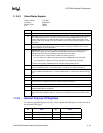
Bit Description
7:0 APM Control Port (APMC). Writes to this register store data in the APMC Register and reads
return the last data written. In addition, writes generate an SMI, if the APMC_EN bit (PCI
Function 3, offset58h, bit 25) is set to 1. Reads do not generate an SMI.