Intel® 460GX Chipset Software Developer’s Manual 9-3
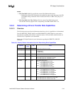
IFB Register Mapping
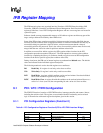
9.2 IDE Configuration
The IFB PCI function 1 contains an IDE Controller capable of standard Programmed I/O (PIO)
transfers as well as Bus Master transfer capability. It also supports the “Ultra DMA/33”
synchronous DMA mode of data transfer.
9.2.1 PCI Configuration Registers (Function 1)
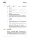
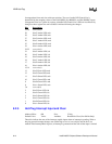
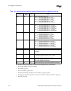
Table 9-2. PCI Configuration Registers–Function 1 (IDE Interface)
Configuration Offset Mnemonic Register Register Access
00–01h VID Vendor Identification RO
02–03h DID Device Identification RO
04–05h PCICMD PCI Command R/W
06–07h PCISTS PCI Device Status R/W
08h RID Revision Identification RO
09-0Bh CLASSC Class Code RO
0Ch – Reserved –
0Dh MLT Master Latency Timer R/W
0Eh HEDT Header Type RO
0F–1Fh – Reserved –
20–23h BMIBA Bus Master Interface Base Address R/W
24–3Fh – Reserved –
40–43h IDETIM IDE Timing R/W
44h SIDETIM Slave IDE Timing R/W
45–47h – Reserved –
48h SDMACTL Synchronous DMA Control R/W
49h – Reserved –
4A–4Bh SDMATIM Synchronous DMA Timing R/W
4C–F7h – Reserved –
F8-FBh --- Manufacturer’s ID ---
FC-FFh --- Reserved ---


