


Intel® 460GX Chipset Software Developer’s Manual 2-45
Register Descriptions
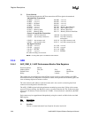
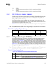
15:8 XTPR 1
These bits represent the external task priority for symmetric agent ID 01h.
7:0 XTPR 0
These bits represent the external task priority for symmetric agent ID 00h.
2.6.2 PID PCI Memory-mapped Registers
The PID uses two 32-bit memory-mapped registers to provide the indirect addressing access to its
(x)APIC interrupt redirection registers as well as to its ID, version, and arbitration ID registers. The
memory-mapped registers are placed at default addresses of FEC0_0000h, FEC0_0010h, and
FEC0_0040h for (x)APIC compatibility.
The I/O select register is used to provide the index of the internal register being accessed. The
register being accessed is determined by bits 7 through 0 of this register. The I/O window register is
used to provide/receive data associated with the access.
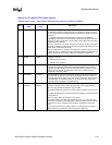
Table 2-2 summarizes the memory-mapped registers. Detailed descriptions of each register follow.
Note: The default base address FEC00 which is mapped to A[31:12] can be changed by reprogramming
the (x)APIC base address register via PCI configuration space access.
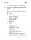
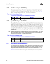
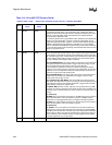
2.6.2.1 I/O Register Select Register (FEC00000h)
The I/O register select register selects which indirect access register appears in the I/O window
register where it can be manipulated by software. The selector values for the indirect access
registers are listed in Section 2.6.3. Software programs bits 7 through 0 of this register to select the
desired internal register. The contents of the selected 32-bit register can be manipulated via the I/O
window register. The I/O register select register is read/write by software and its default is listed in
Section 2.6.2.2. This starting address, where the I/O register select register and I/O window register
reside, can be relocated to a different address via the APIC base address register. The format of the
I/O register select register is shown in Table 2-3.
Note: This register is defined as a 32-bit register, but only the lower eight bits are used. This register must
be accessed using 32-bit memory reads or writes. Bits 31 through 8 should be set to 0s.
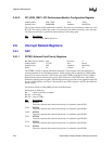
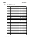
Table 2-2. Memory-Mapped Register Summary
Address Name Access Default Value
FEC00000h I/O Register Select Register R/W 00000000h
FEC00010h I/O Window Register R/W 00000000h
FEC00040h (x)APIC EOI Register R/W 00000000h
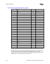
Table 2-3. I/O Select Register Format
Register Offset: FEC00000hDefault Value: [00000000h]Attribute: Read/Write
Bit(s) Name Description
31:8 Reserved These 24 bits are reserved.
7:0 REGISTER
ADDRESS
These eight bits provide the address offset of the internal 32-bit register. This
number is used to select consecutive 32-bit internal registers via the I/O
window register. Described in Section 2.6.2.2 is 64-bit register access.