Intel® 460GX Chipset Software Developer’s Manual 15-15
PCI/LPC Bridge Description
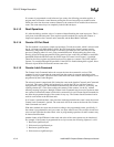
The extended RAM bank is also accessed using an indexed scheme. I/O address 72h is used as the
address pointer and I/O address 73h is used as the data register. Index addresses above 127h are not
valid.
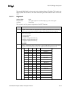
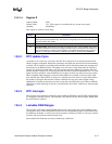
15.5.1.1 Register A
Address Offset: 0Ah
Default Value: NA - This register is not affected by any system reset signal.
Attribute: Read/Write
This register is used for general configuration of the RTC Functions.
Bit(s) Description
7 UPDATE IN PROGRESS (UIP): This bit may be monitored as a status flag. When asserted as a 1,
the update is soon to occur or is in progress. If 0, the update cycle will not start for at least 244 µs.
The time, calendar, and alarm information in RAM is always available when the UIP bit is 0.
6:4 Division Chain Select (DVx): These three bits control the divider chain for the oscillator.
DV2 DV1 DV0 Function
0 1 0 Normal Operation
1 1 X Divider Reset
1 0 1 Bypass 15 stages (test mode only)
1 0 0 Bypass 10 stages (test mode only)
0 1 1 Bypass 5 stages (test mode only)
0 1 1 Invalid
0 0 0 Invalid
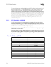
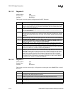
3:0 Rate Select Bits (RSx): Selects one of 13 taps of the 15 stage divider chain. The selected tap can
generate a periodic interrupt if the PIE bit is set in register B. Otherwise this tap will set the PF flag
of register C. If the periodic interrupt is not to be used, these bits should all be set to zero.
RS3 RS2 RS1 RS0 Periodic Rate
0 0 0 0 Interrupt never toggles
0 0 0 1 3.90625 ms
0 0 1 0 7.8125 ms
0 0 1 1 122.070 µs
0 1 0 0 244.141 µs
0 1 0 1 488.281 µs
0 1 1 0 976.5625µs
0 1 1 1 1.953125 ms
1 0 0 0 3.90625 ms
1 0 0 1 7.8125 ms
1 0 1 0 15.625 ms
1 0 1 1 31.25 ms
1 1 0 0 62.5 ms
1101 125 ms
1110 250 ms
1111 500 ms


