LPC/FWH Interface Configuration
11-28 Intel® 460GX Chipset Software Developer’s Manual
11.2.4 NMI Registers
The NMI logic incorporates two different 8-bit registers. The CPU reads the NMISC Register to
determine the NMI source (bits set to a 1). After the NMI interrupt routine processes the interrupt,
software clears the NMI status bits by setting the corresponding enable/disable bit to a 1. The NMI
Enable and Real-Time Clock Register can mask the NMI signal and disable/enable all NMI
sources.
To ensure that all NMI requests are serviced, the NMI service routine software flow should be as
follows:
1. NMI is detected by the processor on the rising edge of the NMI input.
2. The processor will read the status stored in port 061h to determine what sources caused the
NMI. The processor may then set to 0 the register bits controlling the sources that it has
determined to be active. Between the time the processor reads the NMI sources and sets them
to a 0, an NMI may have been generated by another source. The level of NMI will then remain
active. This new NMI source will not be recognized by the processor because there was no
edge on NMI.
3. The processor must then disable all NMIs by setting bit 7 of port 070H to a 1 and then enable
all NMIs by setting bit 7 of port 070H to a 0. This will cause the NMI output to transition low
then high if there are any pending NMI sources. The CPU’s NMI input logic will then register
a new NMI.
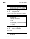
11.2.4.1 Nmisc–Nmi Status and Control Register (I/O)
I/O Address: 061h
Default Value: 00h
Attribute: Read/Write
This register reports the status of different system components, controls the output of the speaker
counter (Counter 2), and gates the counter output that drives the SPKR signal.
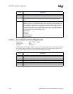
Bit Description
7 SERR# NMI Source Status–RO. Bit 7 is set if a system board agent (PCI devices or main
memory) detects a system board error and pulses the PCI SERR# line. This interrupt source is
enabled by setting bit 2 to 0. To reset the interrupt, set bit 2 to 0 and then set it to 1. When writing
to port 061h, bit 7 must be 0.
6 reserved (0)
5 Timer Counter 2 OUT Status–RO. The Counter 2 OUT signal state is reflected in bit 5. The
value on this bit following a read is the current state of the Counter 2 OUT signal. Counter 2
must be programmed following a CPURST for this bit to have a determinate value. When writing
to port 061h, bit 5 must be a 0.
4 Refresh Cycle Toggle–RO. The Refresh Cycle Toggle signal toggles from either 0 to 1 or 1 to 0
following every refresh cycle. When writing to port 061h, bit 4 must be a 0.
3 Must be programmed to ‘1’.
2 PCI SERR# Enable–R/W. 1=Clear and Disable; 0=Enable.
For the IFB, the SERR# signal can be for a special protocol between the host-to-PCI bridge and
the IFB (see MSTAT Register description, 6Ah-6Bh, Function 0).
1 Speaker Data Enable–R/W. 0=SPKR output is 0; 1= the SPKR output is the Counter 2 OUT
signal value.
0 Timer Counter 2 Enable–R/W. 0=Disable; 1=Enable.


