Intel® 460GX Chipset Software Developer’s Manual 11-41
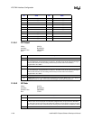
LPC/FWH Interface Configuration
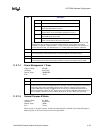
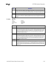
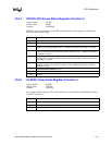
11.2.9.7 GP SMI
Offset: 1C-1Fh
Attribute: Read/Write
Default Value: 00000000h
Size: 32 bits
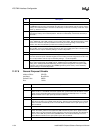
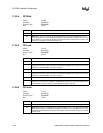
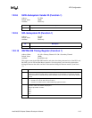
11.2.9.8 GP Pulse
Offset: 20-23h
Attribute: Read/Write
Default Value: 00000000h
Size: 32 bits
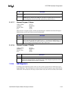
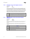
11.2.9.9 GP Core
Offset: 24-27h
Attribute: Read/Write
Default Value: 00000000h
Size: 32 bits
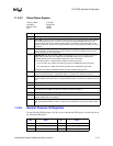
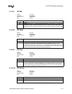
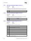
11.2.9.10 GP Pull-up
Offset: 28-2Bh
Attribute: Read/Write
Default Value: 03FFh
Size: 32 bits
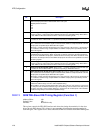
Bit Description
31:9 Reserved.
8:0 SMI Rout: When set to a ‘1’, and the corresponding data bit is set to an input, a ‘1’ in the data bit
register will be routed to an SMI. If the data bit is set to an output, this value of this bit has no
effect. When cleared, no routing is performed. This bit cannot be changed once the GP Lock bit
is set.
Bit Description
31:9 Reserved.
8:0 Pulse: When set to a ‘1’, and the data bit (after the invert bit) is programmed as an input, a ‘0’ to
‘1’ transition that is longer than 2 RTC clocks will cause the data bit to be set. A ‘1’ to ‘0’
transition will not clear the bit. Only a write of ‘1’ to the data bit can clear the data bit. If the data
bit is not set to an output, this value of this bit has no effect. When cleared, edge triggering is not
performed. This bit cannot be changed once the GP Lock bit is set.
Bit Description
31:9 Reserved.
8:0 Core: When set to a ‘1’, and the data bit is programmed as an output, a ‘0’ will be driven on the
pin when core power loss is detected (PWROK low). This allows the pin, while in the resume
well, to be connected to a device in the core well. When cleared, this check is not performed.
This bit cannot be changed once the GP Lock bit is set.
Bit Description
31:10 Reserved.
9:0 Pull-up: When set, an internal pull-up will be enabled on the pin. When disabled, the pull-up is
disabled. This bit cannot be changed once the GP Lock bit is set.


