Intel® 460GX Chipset Software Developer’s Manual 12-7
IDE Configuration
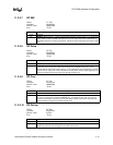
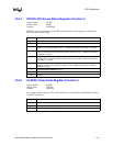
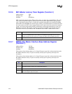
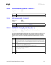
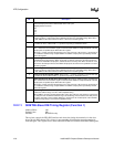
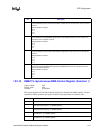
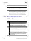
12.2.12 DMACTL–Synchronous DMA Control Register (Function 1)
Address Offset: 48h
Default Value: 00h
Attribute: Read/Write
This register enables each individual channel and drive for Synchronous DMA transfers. For non-
synchronous DMA operation, this register should be left programmed to its default value.
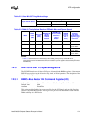
Bit Description
7:6 Secondary Drive 1 IORDY Sample Point (SISP1). This field selects the number of PCI clocks
between SDIOx# assertion and the first SIORDY sample point for the slave drive on the secondary
channel.
Bits[7:6] Number of Clocks
00 5
01 4
10 3
11 2
5:4 Secondary Drive 1 Recovery Time (SRTC1). This field selects the minimum number of PCI
clocks between the last SIORDY# sample point and the SDIOx# strobe of the next cycle for the
slave drive on the secondary channel.
Bits[5:4] Number of Clocks
00 4
01 3
10 2
11 1
3:2 Primary Drive 1 IORDY Sample Point (PISP1). This field selects the number of PCI clocks
between PDIOx# assertion and the first PIORDY sample point for the slave drive on the primary
channel.
Bits[3:2] Number of Clocks
00 5
01 4
10 3
11 2
1:0 Primary Drive 1 Recovery Time (PRTC1). This field selects the minimum number of PCI clocks
between the last PIORDY# sample point and the PDIOx# strobe of the next cycle for the slave
drive on the primary channel.
Bits[1:0] Number of Clocks
00 4
01 3
10 2
11 1
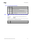
Bit Description
7:4 Reserved.
3 Secondary Drive 1 SDMA Enable (SSDE1). 1 = Enable Synchronous DMA mode for
secondary channel drive 1. 0 = Disable (default).
2 Secondary Drive 0 SDMA Enable (SSDE0). 1 = Enable Synchronous DMA mode for
secondary channel drive 0. 0 = Disable (default).
1 Primary Drive 1 SDMA Enable (PSDE1). 1 = Enable Synchronous DMA mode for primary
channel drive 1. 0 = Disable (default).
0 Primary Drive 0 SDMA Enable (PSDE0). 1 = Enable Synchronous DMA mode for primary
channel drive 0. 0 = Disable (default).


