


Intel® 460GX Chipset Software Developer’s Manual 14-3
SM Bus Controller Configuration
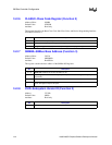
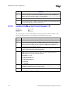
14.2.4 PCISTS–PCI Device Status Register (Function 3)
Address Offset: 06-07h
Default Value: 0280h
Attribute: Read/Write
DSR is a 16-bit status register that reports the occurrence of a PCI target-abort when the System
Management Function is a target device. The register also indicates the System Management
DEVSEL# signal timing that is hardwired in the module. The DSR fields are shown in the table
below.
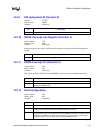
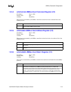
14.2.5 RID–Revision Identification Register (Function 3)
Address Offset: 08h
Default Value: Initial Stepping = 00h. Refer to IFB Specification Updates
for other values programmed here.
Attribute: Read only
This 8 bit register contains device stepping information. Writes to this register have no effect.
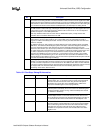
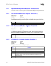
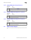
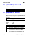
1 Memory Space Enable (Not Implemented). 1=Enable. 0=Disable. This bit controls the access to
memory space. If this bit is set, access to the memory space by power management logic is
enabled.
0 I/O Space Enable (IOSE). 1=Enable. 0=Disable. This bit controls the access to the I/O space
registers. If this bit is set, access to the power management I/O registers is enabled. The base
register for the I/O registers must be programmed before this bit is set.
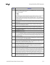
Bit Description
Bit Description
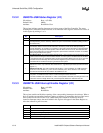
15 Detected Parity (Not Implemented). This bit is hardwired to 0.
14 SERR# Status (Not Implemented). This bit is hardwired to 0.
13 Master-Abort Status (Not Implemented). This bit is hardwired to 0.
12 Received Target-Abort Status (Not Implemented). This bit is hardwired to 0.
11 Signaled Target-Abort Status (STA)–R/WC. This bit is set when the Power Management
Function is targeted with a transaction that the it terminates with a target abort. Software resets
STA to 0 by writing a 1 to this bit.
10:9 DEVSEL# Timing Status (DEVT)–RO. This 2-bit field defines the timing for DEVSEL#
assertion. These read only bits indicate the IFB’s DEVSEL# timing when performing a positive
decode. Since the IFB always generate the DEVSEL# with medium timing, DEVT=01. This
DEVSEL# timing does not include Configuration cycles.
8 Data Parity Detected (Not Implemented). This bit is hardwired to 0.
7 Fast Back to Back Capable (FBC)–RO. Hardwired to 1. This bit indicates to the PCI Master
that Power Management as a target is capable of accepting fast back-to-back transactions.
6:0 Reserved. Read as 0’s.
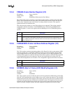
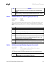
Bit Description
7:0 Revision ID Byte. The register is hardwired to the default value.