Intel® 460GX Chipset Software Developer’s Manual 2-19
Register Descriptions
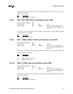
5 Memory Bus A ECC correction/detection enable.
4 Memory Bus B ECC correction/detection enable.
3:0 Double byte parity mask for 128 bits of data.
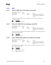
2.4.2.23 PVD_D_FERR: Data on First PVD Parity Error
Bus CBN, Device Number: 04h
Address Offset: D0-D7h Size: 64 bits
Default Value: 0 Attribute: Read Only, New Value Latched
anytime appropriate FERR register
bit is set
This register records and latches the data associated with the first parity error detected on the PVD
bus.
Bits
Description
63:0 PVD - Private Data Bus data.
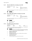
2.4.2.24 PVD_PAR_FERR: Parity on First PVD Parity Error
Bus CBN, Device Number: 04h
Address Offset: D8h Size: 8 bits
Default Value: 0 Attribute: Read Only, New Value Latched
anytime appropriate FERR register
bit is set
This register records and latches the data associated with the first parity error detected on the PVD
bus.
Bits
Description
7:4 reserved(0)
3:0 Double–byte parity of error
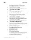
2.4.2.25 PVD_TXINFO_FERR: TXINFO on First PVD Parity Error
Bus CBN, Device Number: 04h
Address Offset: D9-DAh Size: 16 bits
Default Value: 00h Attribute: Read Only, New Value Latched
anytime appropriate FERR register
bit is set
This register records the ITID and failing chunk corresponding to the first double-byte parity
detected by private bus interface in the SDC.
Bits
Description
15:9 reserved(0)
8:6 DC - Data Chunk of ITID.
5:0 ITID - ITID of error.


