Register Descriptions
2-26 Intel® 460GX Chipset Software Developer’s Manual
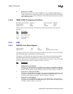
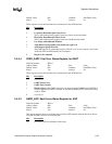
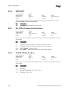
2.4.5.6 NERR_GART
Function Number: BFN+1
Address Offset: 8Eh Size: 8 bits
Default Value: 00h each Attribute: Read/Write Clear
Sticky: Yes Locked: No
This register records all error conditions detected in the GART logic after the first error. Errors
recorded in FERR_GART are not recorded here.
Bits
Description
7:0 See FERR_GART for definitions of these bits.
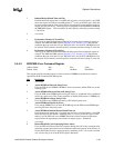
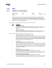
2.4.5.7 PAC_ERR: PCI Address & Cmd First Error
Function Number: BFN+1
Address Offset: A0h Size: 64 bits
Default Value: 0000000000h each Attribute: Read/Write
Sticky: Yes Locked: No
These registers record and latch the Address and Command information on the PCI Bus for the first
error detected.
Bits
Description
63:46 reserved(0)
45 PCI Parity (2nd phase of DAC, not defined for non-DAC address).
44 PCI Parity (if DAC, this is the parity of the first half of the address).
43:40 PCI Command - Command of Error.
39:0 PCI Address - Address Received on Error. (possible DAC address).
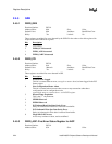
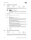
2.4.5.8 PD_ERR: PCI Data First Error
Function Number: BFN+1
Address Offset: A8h Size: 64 bits
Default Value: 00h each Attribute: Read/Write
Sticky: Yes Locked: No
These registers record and latch the Data and Byte Enable information on the PCI Bus for the first
error detected.
Bits
Description
63:37 reserved(0)
36 PCI Parity.
35:32 PCI Byte Enable [3:0] - Byte Enable of Error.
31:0 PCI Data - Data of Error.


