IDE Configuration
12-2 Intel® 460GX Chipset Software Developer’s Manual
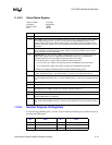
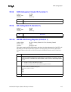
12.2.1 VID–Vendor Identification Register (Function 1)
Address Offset: 00–01h
Default Value: 8086h
Attribute: Read only
The VID Register contains the vendor identification number. This register, along with the Device
Identification Register, uniquely identifies any PCI device. Writes to this register have no effect.
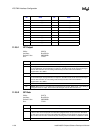
12.2.2 DID–Device Identification Register (Function 1)
Address Offset: 02–03h
Default Value: 7601h
Attribute: Read only
The DID Register contains the device identification number. This register, along with the VID
Register, defines the IFB Function. Writes to this register have no effect.
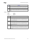
12.2.3 PCICMD–PCI Command Register (Function 1)
Address Offset: 04–05h
Default Value: 0000h
Attribute: Read/Write
The PCICMD Register controls access to the I/O space registers.
Bit Description
15:0 Vendor Identification Number. This is a 16-bit value assigned to Intel
Bit Description
15:0 Device Identification Number. This is a 16-bit value assigned to the IFB IDE Controller Function.
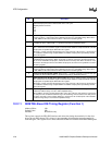
Bit Description
15:10 Reserved.
9 Fast Back to Back Enable (FBE). This bit is hardwired to 0.
8 SERR# Enable. This bit is hardwired to 0.
7 Wait Cycle Control. This bit is hardwired to 0.
6 Parity Error Response. This bit is hardwired to 0.
5 VGA Palette Snoop. This bit is hardwired to 0.
4 Postable Memory Write and Invalidate Enable. This bit is hardwired to 0.
3 Special Cycle Enable. This bit is hardwired to 0.
2 Bus Master Function Enable (BME). 1=Enable. 0=Disable.
1 Memory Space Enable. This bit is hardwired to 0.
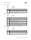
0 I/O Space Enable (IOSE). This bit controls access to the I/O space registers. When IOSE=1,
access to the Legacy IDE ports (both primary and secondary) and the PCI Bus Master IDE I/O
Registers is enabled. The Base Address Register for the PCI Bus Master IDE I/O Registers should
be programmed before this bit is set to 1.


