Intel® 460GX Chipset Software Developer’s Manual 2-17
Register Descriptions
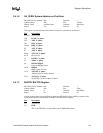
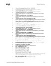
This register records and latches the data associated with the first parity error detected on the
PITID bus.
Bits
Description
7 If set then the error was detected on the 1
st
half of the double-pumped transfer. Otherwise,
these fields contain the information from the 2
nd
half of the double-pumped transfer.
6 Parity of Error
5:0 PITID - Private ITID bus value of Error.
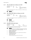
2.4.2.17 SDCRSP_FERR: Response on First SDCRSP Error
Bus CBN, Device Number: 04h
Address Offset: 8Dh Size: 8 bits
Default Value: 0h Attribute: Read Only, New Value Latched
anytime appropriate FERR register
bit is set
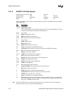
This register records and latches the data and inverted data associated with the first transmission
error detected on the SDCRSP bus.
Bits
Description
7:4 Response Bus for 2
nd
half of double–pumped transfer.
3:0 Response Bus for 1
st
half of double–pumped transfer.
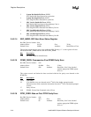
2.4.2.18 DPBRLE_FERR: Private Data Bus Receive Length Error
Bus CBN, Device Number: 04h
Address Offset: 8Eh Size: 8 bits
Default Value: 0h Attribute: Read Only, New Value Latched
anytime appropriate FERR register
bit is set
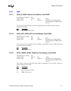
This register indicates that the amount of data transferred from the SAC to the SDC for a given
transfer did not match the expected transfer length.
Bits
Description
7:3 reserved(0)
2 Data packet longer than expected (LDP)
1 Data packet shorter than expected (SDP)
0 No data packet shipped as expected (NDP)
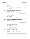
2.4.2.19 ECCMSK0: ECC Mask Register - Card B
Bus CBN, Device Number: 04h
Address Offset: C8h Size: 8 bits
Default Value: 00h Attribute: Read/Write
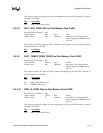
This register is used to test the ECC error detection logic in the memory subsystem for memory
card 0. To test, this register is written with a masking function. All subsequent writes into memory
will store a masked version of the computed ECC. Subsequent reads of memory locations written


