LPC/FWH Interface Configuration
11-40 Intel® 460GX Chipset Software Developer’s Manual
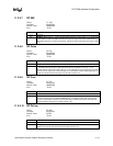
11.2.9.4 GP Blink
Offset: 0C-0Fh
Attribute: Read/Write
Default Value: 00000000h
Size: 32 bits
11.2.9.5 GP Lock
Offset: 10-13h
Attribute: Read/Write
Default Value: 00000000h
Size: 32 bits
11.2.9.6 GP Invert
Offset: 14-17h
Attribute: Read/Write
Default Value: 00000000h
Size: 32 bits
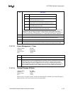
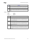
Bit Description
31:9 Reserved.
8:0 Blink: When set to a ‘1’, and the GP pin is programmed as an output, it will blink at a rate of
once per second. The value of the data bit remains unchanged during the blink process. If it was
set, it remains set. The setting of this bit has no effect if the pin is programmed as an input. This
bit cannot be changed once the GP Lock bit is set.
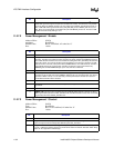
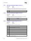
Bit Description
31:29 Reserved.
28:24 Muxed Lock: When set, and the pin is programmed as an output, the data bit cannot be
changed. Once this bit is set, it can only be cleared by a PCIRST#. Once this bit is set, all other
register bits at this bit location cannot be changed.
23:20 Reserved.
19:16 Muxed Lock: When set, and the pin is programmed as an output, the data bit cannot be
changed. Once this bit is set, it can only be cleared by a PCIRST#. Once this bit is set, all other
register bits at this bit location cannot be changed.
15:9 Reserved.
8:0 Lock: When set, and the pin is programmed as an output, the data bit cannot be changed. Once
this bit is set, it can only be cleared by a PCIRST#. Once this bit is set, all other register bits at
this bit location cannot be changed. This is applicable to GPO mode only.
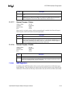
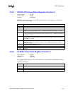
Bit Description
31:9 Reserved.
8:0 Invert: When set to a ‘0’, the GPIO pin is not inverted. When set to ‘1’, the GPIO pin is inverted.
When set to an output, the data bit is inverted before it is driven on the pin. When set to an input,
the data bit is inverted before entering the data register. This bit cannot be changed once the GP
Lock bit is set.


