


Intel® 460GX Chipset Software Developer’s Manual 11-39
LPC/FWH Interface Configuration
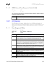
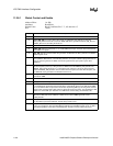
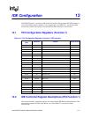
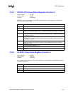
11.2.9.3 GP TTL
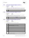
Offset: 08-0Bh
Attribute: Read/Write
Default Value: 00000000h
Size: 32 bits
19:16 Muxed Data: If a data bit is programmed to be an output, then this bit can be updated by software
to drive a value on the output pin. If the data bit is programmed as an input, then this bit reflects
the state of the input pin and cannot be updated by software. This bit cannot be changed once the
GP Lock bit is set. The value of this bit only has meaning if the muxed GPIO is enabled as a GPIO.
15:9 Reserved.
8:0 Data: If a data bit is programmed to be an output, then this bit can be updated by software to drive
a value on the output pin. If the data bit is programmed as an input, then this bit reflects the state
of the input pin and cannot be updated by software. This bit cannot be changed once the GP Lock
bit is set.
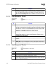
Bit Description
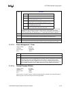
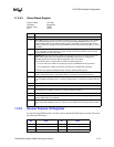
Bit Description
31:29 Reserved.
28:24 Muxed TTL: When set to a ‘1’, and the data bit is programmed as an output, the pin will be
driven with the value of the pin. When set to a ‘0’, and the data bit is programmed as an output,
the pin will be tri-stated when the pin is to be driven to a ‘1’, and driven when the pin is to be
driven to a ‘0’. The setting of this bit has no effect if the pin is programmed as an input. This bit
cannot be changed once the GP Lock bit is set. The value of this bit only has meaning if the
muxed GPIO is enabled as a GPIO.
23:20 Reserved.
19:16 Muxed TTL: When set to a ‘1’, and the data bit is programmed as an output, the pin will be
driven with the value of the pin. When set to a ‘0’, and the data bit is programmed as an output,
the pin will be tri-stated when the pin is to be driven to a ‘1’, and driven when the pin is to be
driven to a ‘0’. The setting of this bit has no effect if the pin is programmed as an input. This bit
cannot be changed once the GP Lock bit is set. The value of this bit only has meaning if the
muxed GPIO is enabled as a GPIO.
15:9 Reserved.
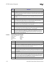
8:0 TTL: When set to a ‘1’, and the data bit is programmed as an output, the pin will be driven with
the value of the pin. When set to a ‘0’, and the data bit is programmed as an output, the pin will
be tri-stated when the pin is to be driven to a ‘1’, and driven when the pin is to be driven to a ‘0’.
The value of the pin is determined by XORing the data bit with the invert bit. The setting of this
bit has no effect if the pin is programmed as an input. This bit cannot be changed once the GP
Lock bit is set.