


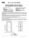

Silicon Gate MOS
8702A
2048
BIT ERASABLE AND ELECTRICALLY
REPROGRAMMABLE READ ONLY MEMORY
• Inputs and Outputs TTL Compatible
• Three-State Output - OR-Tie
Capability
• Simple Memory Expansion Chip
Select Input Lead
• Access Time
-1.3
~sec
Max.
• Fast Programming - 2 Minutes for
All
2048
Bits
• Fully Decoded,
256
x 8 Organization
• Static MOS - No Clocks Required
The 8702A
is
a 256 word
by
8
bit
electrically programmable
ROM
ideally suited
for
microcomputer system
development where fast turn-around and pattern experimentation
are
important. The
8702A
undergoes
complete programming and functional testing on
each
bit
position
prior
to
shipment, thus insuring 100%
programmability.
The 8702A
is
packaged in a 24 pin dual-in line package
with
a transparent quartz lid. The transparent quartz
lid allows the
user
to
expose the chip
to
ultraviolet light
to
erase
the
bit
pattern. A new pattern
can
then
be
written
into
the device. This procedure
can
be
repeated
as
many times
as
required.
The circuitry
of
the
8702A
is
entirely static; no clocks
are
required.
A pin-for-pin metal
mask
programmed ROM, the Intel 8302,
is
ideal
for
large volume production runs
~f
systems
initially
using the
8702A.
The
8702A
is
fabricated
with
silicon gate technology. This
low
threshold technology allows the design and
production
of
higher performance MOS circuits and provides a higher functional density on a
monolithic
chip than conventional MOS technologies.
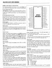
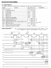
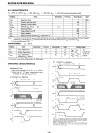
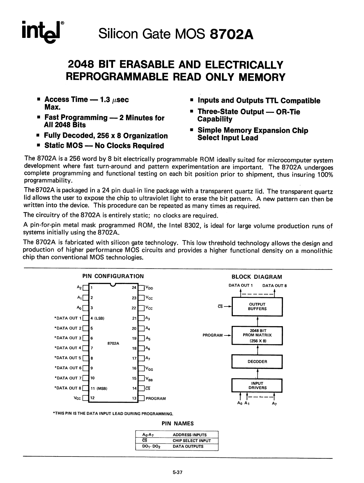
PIN
CONFIGURATION
BLOCK
DIAGRAM
OUTPUT
BUFFERS
2048
BIT
PROM
MATRIX
(256 X
8)
DATA
OUT 1
DATA
OUT 8
PROGRAM
........
A
2
V
oo
A,
Vee
Ao
Vee
*DATA
OUT 1
A
3
*DATA
OUT 2
A
4
*DATA
OUT 3
As
*DATA
OUT 4
A
6
*DATA
OUT 5
A
7
*DATA
OUT 6
9
16
V
GG
*DATA
OUT 7
10
15
Vee
*DATA
OUT 8
11
(MSB)
14
CS
Vee
12
13
PROGRAM
*THIS
PIN
IS
THE
DATA
INPUT LEAD DURING PROGRAMMING.
PIN NAMES
Ao-A7
ADDRESS INPUTS
CS
CHIP SELECT INPUT
001-
002
DATA
OUTPUTS
5-37