


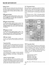
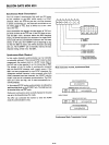
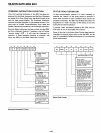
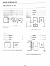


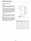
SILICON GATE MOS 8251
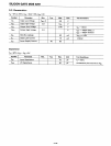
A.C. Characteristics:
TA
=
o°c
to
70°C;
VCC
= 5.0V
±5%;
Vss =
OV
Symbol
Parameter Min.
Typ.
Max.
Unit
Test Conditions
tCY
Clock Period .420
1.35
JlS
t</JW
Clock Pulse Width 220 300
ns
tR,tF
Clock
Rise
and Fall Time
0
50
ns
tWR
WRITE Pulse Width
430
ns
tos
Data Set-Up Time for
WR
ITE
0
ns
tOH
Data
Hold
Time for
WR
ITE
65
ns
tAW
Address Stable before
WR
ITE
20
ns
tWA
Address
Hold
Time for
WR
ITE
35
ns
tRO
READ
Pulse Width
430 ns
too
Data Delay from READ 350
ns
CL=100pF
tOF
READ
to
Data Floating
150
ns
Cl=100pF
tAR1
Address Stable before READ,
CE
(C/D)
50 ns
tRA1
Address Hold Time for READ,
CE
5
ns
tRA2
Address Hold Time for READ,
C/O
370 ns
tOTx
TxD Delay from Falling
Edge
of TxC
1
JlS
CL=100pF
tSRx
Rx
Data Set-Up Time
to
Sampling Pulse
2
J.l.S
Cl=100pF
tHRx
Rx
Data Hold Time
to
Sampling Pulse
2
J.l.S
CL=100pF
fTx
Transmitter Input Clock Frequency
1X Baud Rate
DC
56
KHz
16X and 64X Baud Rate
DC
615
KHz
fRx
Receiver Input Clock Frequency
1X
Baud
Rate
DC
56
KHz
16X and 64X Baud Rate
DC
615
KHz
tTx
TxRDY Delay from Center of Data Bit
16
ClK
Period
CL
=50pF
tRx
RxRDY Delay from Center of Data
Bit
15
20
ClK
Period
tiS
Internal Syndet Delay from Center of Data
Bit
20 25
ClK
Period
tES
External Syndet Set-Up Time before Falling
15
ClK
Period
Edge
of RxC
Note:
The
TxC
and
Rxe
frequencies
have
the
following
I
imitation
with
respect
to
ClK.
For
ASYNC
Mode,
tTx
or
tRx
~
4.5
tCY
For
SYNC
Mode,
tTx
or
tRx
~
30
tCY
5-145