


with a clearly defined activity
is
called a State. And
the
inter-
val
between pulses
of
the
timing oscillator
is
referred
to
as a
Clock Period. As a general rule,
one
or
more clock periods
are necessary
for
the
completion
of
a state, and there are
several states
in
a cycle.
Instruction Fetch:
The
first state(s)
of
any
instruction cycle will be
dedicated
to
fetching
the
next
instruction.
The
CPU issues a
read signal and
the
contents
of
the
program
counter
are sent
to
memory, which responds
by
returning
the
next
instruc-
tion
word. The first
byte
of
the
instruction
is
placed
in
the
instruction register.
If
the
instruction consists
of
more
than
one
byte, additional states are required
to
fetch each byte
of
the
instruction. When
the
entire instruction
is
present
in
the
CPU,
the
program
counter
is
incremented (in prepara-
tion for
the
next
instruction fetch) and
the
instruction
is
decoded.
The
operation specified
in
the
instruction will be
executed in
the
remaining states
of
the
instruction cycle.
The instruction may call for a memory read
or
write, an
input
or
output
and/or
an internal CPU operation, such
as
a register-to-register transfer
or
an add-registers operation.
Memory Read:
An instruction
fetch
is
merely a special memory read
operation
that
brings
the
instruction
to
the
CPU's instruc-
tion register. The instruction fetched may
then
call for data
to
be read from memory into
the
CPU.
The
CPU
again issues
a read signal and sends
the
proper memory address; memory
responds by returning
the
requested
word.
The
data
re-
ceived
is
placed
in
the
accumulator
or
one
of
the
other
gen-
eral purpose registers
(not
the
instruction register).
Memory Write:
A memory write operation
is
similar
to
a read except
-for
the
direction
of
data
flow.
The
CPU issues a write
signal, sends
the
proper memory address,
then
sends
the
data
word
to
be written into
the
addressed memory location.
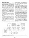
Wait (memory synchronization):
As previously stated,
the
activities
of
the
processor
are
timed
by a master clock oscillator.
The
clock period
determines
the
timing
of
all processing activity.
The
speed
of
the
processing cycle, however,
is
limited
by
the
memory'sAccess Time. Once
the
processor has sent a
read address
to
memory, it
cannot
proceed until
the
memory
has had time
to
respond. Most memories are capable
of
responding much faster
than
the
processing cycle requires.
A few, however,
cannot
supply
the
addressed byte within
the
minimum time established by
the
processor's clock.
Therefore a processor should contain a synchroniza-
tion
provision, which permits
the
memory
to
request a Wait
state. When
the
memory rec.eives a read
or
write enable
sig-
nal, it places a request signal
on
the
processor's READY line,
causing
the
CPU
to
idle temporarily.
After
the
memory has
1-4
had time
to
respond, it frees
the
processor's READY line,
and
the
instruction cycle proceeds.
Input/Output:
Input and
Output
operations
are similar
to
memory
read and write operations with
the
exception
that
a peri-
pherall/O
device
is
addressed instead
of
a memory location.
The
CPU
issues
the
appropriate
input
or
output
control
signal, sends
the
proper device address and either receives
the
data being
input
or
sends
the
data
to
be
output.
Data can be
input/output
in
either parallel
or
serial
form. All data within a digital
computer
is
represented
in
binary coded form. A binary
data
word
consists
of
a group
of bits; each bit
is
either a
one
or
a zero. Parallel I/O con-
sists
of
transferring all bits
in
the
word
at
the
same time,
one bit per line. Serial I/O consists
of
transferring one
bit
at
a time
on
a single line. Naturally serial I/O
is
much
s.lower,
but
it requires considerably less hardware
than
does
parallel I/O.
Interrupts:
Interrupt. provIsions are included
on
many central
processors, as a means
of
improving
the
processor's effi-
ciency. Consider
the
case
of
a
computer
that
is
processing a
large volume
of
data,
portions
of
which are
to
be
output
to
a printer.
The
CPU can
output
a
byte
of
data
within a
single machine cycle
but
it may
take
the
printer
the
equiva-
lent
of
many machine cycles
to
actually
print
the
character
specified by
the
data
byte. The CPU could
then
remain idle
waiting until
the
printer can accept
the
next
data
byte.
If
an interrupt capability
is
implemented
on
the
computer,
the
CPU
can
output
a
data
byte
then
return
to
data processing.
When
the
printer
is
ready
to
accept
the
next
data
byte, it
can request an interrupt. When
the
CPU acknowledges
the
interrupt, it suspends main program execution and auto-
matically branches
to
a
routine
that
will
output
the
next
data byte.
After
the
byte
is
output,
the
CPU
continues
with main program execution.
Note
that
this
is,
in principle,
quite similar
to
a subroutine call,
except
that
the
jump
is
initiated externally rather
than
by
the
program.
More complex
interrupt
structures are possible,
in
which several interrupting devices share
the
same processor
but
have different priority levels. Interruptive processing
is
an
important
feature
that
enables
maximum
untilization of
a processor's capacity for high system
throughput.
Hold:
Another
important
feature
that
improves
the
through-
put
of
a processor
is
the
Hold.
The
hold provision enables
Direct Memory Access (DMA) operations.
In
ordinary input and
output
operations,
the
processor
itself supervises
the
entire
data
transfer. Information
to
be
placed
in
memory
is
transferred from
the
input
device
to
the
processor, and
then
from
the
processor
to
the
designated
memory location.
In
similar fashion, information
that
goes
_
...