


The
input
level specification impl ies
that
any
semi-
conductor
memory
or
I/O device
connected
to
the
8080
Data Bus
must
be able
to
provide a minimum
of
3.3
volts
in
its high
state.
Most
semiconductor
mem-
ories
and
standard
TTL
I/O devices have an
output
capability
of
between
2.0
and
2.8
volts, obviously a
direct
connection
onto
the
8080
Data Bus would re-
quire pullup resistors,
whose
value should
not
affect
the
bus speed
or
stress
the
drive capability
of
the
memory
or
I/O
components.
The
80S0A
output
drive capability
(lOl)
1.9mA
max.
is
sufficient
for
small systems
where
Memory size
and
I/O
requirements
are minimal
and
the
entire system
is
contained
on
a single
printed
circuit
board. Most sys-
tems
however,
take
advantage
of
the
high-perfor-
mance
computing
power
of
the
8080
CPU
and
thus
a
more typical system
would
require some
form
of
buf-
fering
on
the
80S0
Data Bus
to
support
a larger array
of
Memory and I/O devices which are likely
to
be on
separate boards.
A device specifically designed
to
do
this buffering
function
is
the
INTEL®
8216,
a (4)
four
bit
bi-direc-
tional bus driver whose
input
voltage level
is
compat-
ible
with
standard
TTL
devices
and
semiconductor
memory
components,
and
has
output
drive capability
of
50
mAo
At
the
8080
side,
the
8216
has a
"high"
output
of
3.65
volts
that
not
only
meets
the
S080
input
spec
but
provides
the
designer with a worse case
350
mV noise margin.
A pair
of
S216's
are
connected
directly
to
the
8080
Data Bus
(07-00)
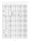
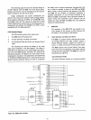
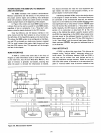
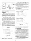
as shown in figure 3-5. Note
that
the
OBI
N signal
from
the
8080
is
connected
to
the
direction control
input
(01 EN) so
the
correct
flow
of
data
on
the
bus
is
maintained.
The
chip
select (CS)
of
the
S216
is
connected
to
BUS ENABLE (BUSEN)
to
allow for DMA activities
by
deselecting
the
Data Bus
Buffer
and
forcing
the
outputs
of
the
S216's
into
their
high impedance
(3-state)
mode. This allows
other
devices
to
gain access
to
the
data
bus (DMA).
System
Control Logic Design
The
Control Bus maintains discipline
of
the
bi-direc-
tional Data Bus,
that
is, it
determines
what
type
of
device will have access
to
the
bus (Memory
or
I/O)
and generates signals
to
assure
that
these
devices
transfer Data
with
the
SOSO
CPU
within
the
proper
timing
"windows"
as
dictated
by
the
CPU operational
characteristics.
As described previously,
the
8080
issues
Status
infor-
mation
at
the
beginning
of
each Machine Cycle
on
its
Data Bus
to
indicate
what
operation
will
take
place
during
that
cycle. A simple (8)
bit
latch, like an
INTEL®
8212,
connected
directly
to
the
80S0
Data
Bus
(07-00)
as shown
in
figure 3-5 will store
the
3-5
Status
information.
The
signal
that
loads
the
data
into
the
Status
Latch
comes
from
the
Clock Gener-
ator,
it
is
Status
Strobe
(STSTB)
and
occurs
at
the
start
of
each Machine Cycle.
Note
that
the
Status
Latch
is
connected
onto
the
SOSO
Data Bus
(07-00)
before
the
Bus Buffer. This
is
to
maintain
the
integrity
of
the
Data Bus
and
simplify
Control
Bus
timing
in DMA
dependent
environments
..
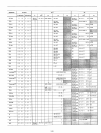
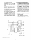
As shown in
the
diagram, a simple gating
of
the
out-
puts
of
the
Status
Latch
with
the
DB
I
Nand
WR
signals
from
the
S080
generate
the
(4)
four
Control
signals
that
make
up
the
basic
Control
Bus.
These
four
signals: 1. Memory Read (MEM
R)
2.
Memory
Write (MEM
W)
3. I/O Read (I/O
R)
4.
I/O Write (I/O
W)
TM
connect
directly
to
the
MCS-80
component
"family"
of
ROMs, RAMs
and
I/O devices.
A fifth signal,
Interrupt
Acknowledge (lNTA)
is
added
to
the
Control
Bus by gating
data
off
the
Status
Latch
with
the
DBIN signal
from
the
S080
CPU. This signal
is
used
to
enable
the
Interrupt
Instruction
Port
which holds
the
RST instruction
onto
the
Data Bus.
Other
signals
that
are
part
of
the
Control
Bus such as
WO,
Stack
and
M1 are
present
to
aid in
the
testing
of
the
System
and
also
to
simplify interfacing
the
CPU
to
dynamic
memories
or
very large
systems
that
re-
quire several levels
of
bus buffering.
Address Buffer Design
The
Address Bus (A15-AO)
of
the
8080,
like
the
Data
Bus,
is
sufficient
to
support
a small system
that
has a
moderate
size Memory
and
I/O
structure,
confined
to
a single card.
To
expand
the
size
of
the
system
that
the
Address Bus
can
support
a simple
buffer
can be
added,
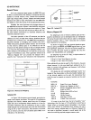
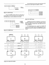
as shown
in
figure 3-6.
The
INTEL®S212
or
8216
is
an
excellent
device
for
this
function.
They
provide low
input
loading
(.25
mA), high
output
drive
and
insert a minimal delay
in
the
System
Timing.
Note
that
BUS ENABLE (BUSEN)
is
connected
to
the
buffers so
that
they
are
forced
into
their
high-
impedance
(3-state)
mode
during
DMA activities so
that
other
devices can gain access
to
the
Address Bus.