


Silicon Gate
MOS
8255
PROGRAMMABLE PERIPHERAL INTERFACE
•
24
Programmable
I/O
Pins
• Completely TTL Compatible
• Fully Comp.atible
with
MCS™-8
and
MCS
TM'_80
Microprocessor Families
• Direct
Bit
Set/Reset
Capability
Easing Control Application Interface
•
40
Pin Dual In-Line Package
• Reduces System Package Count
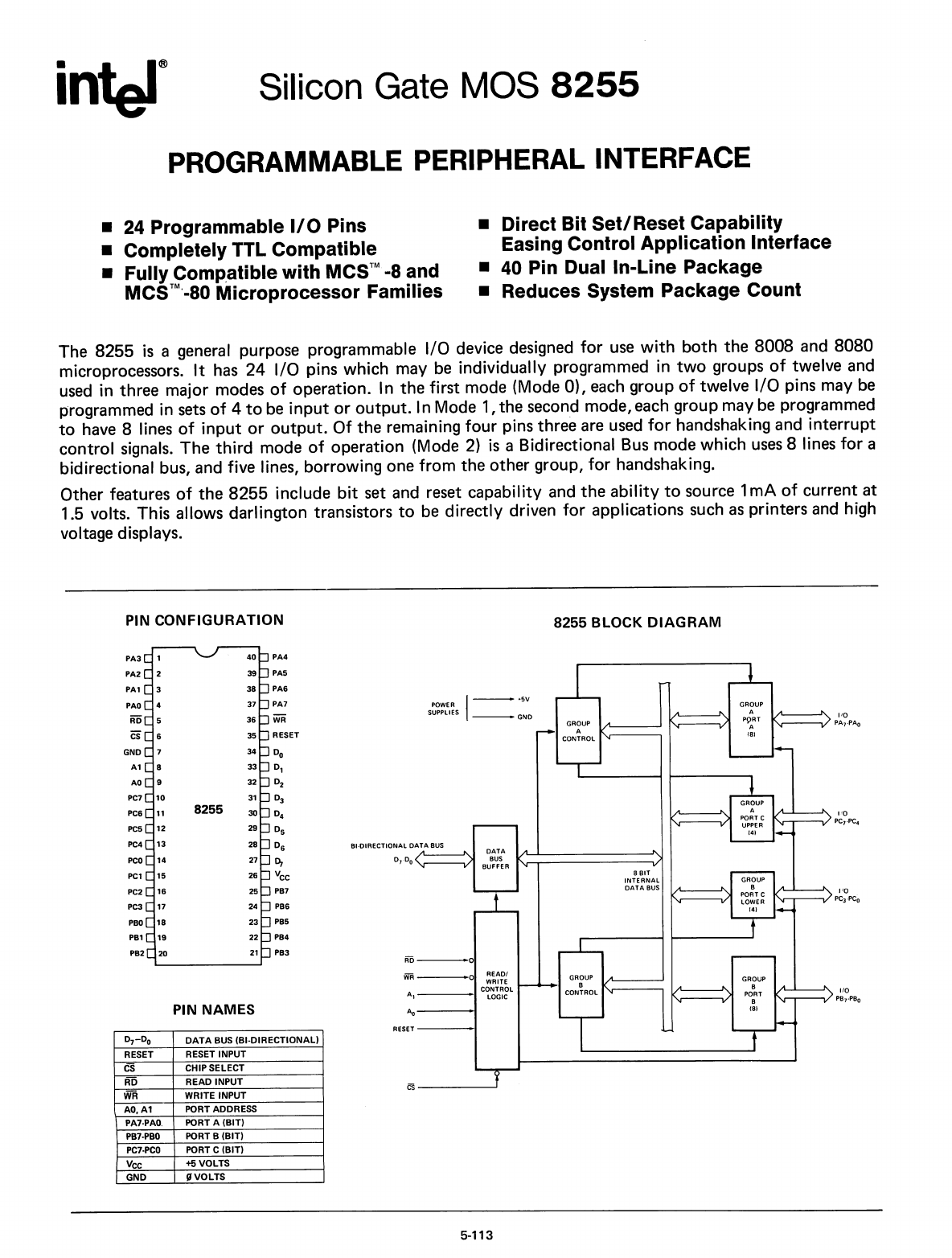
The 8255
is
a general purpose programmable
I/O
device designed
for
use
with
both
the 8008 and 8080
microprocessors.
It
has
24
I/O
pins which may
be
individually programmed in
two
groups
of
twelve and
used
in three major modes
of
operation. In the
first
mode (Mode 0),
each
group
of
twelve
I/O
pins may
be
programmed in
sets
of
4
to
be
input
or
output.
In Mode 1, the second mode,
each
group may
be
programmed
to
have 8 lines
of
input
or
output.
Of
the remaining
four
pins three
are
used
for
handshaking and
interrupt
control
signals. The
third
mode
of
operation (Mode
2)
is
a Bidirectional Bus mode which
uses
8 lines
for
a
bidirectional bus, and five lines, borrowing one
from
the other group,
for
handshaking.
Other features
of
the 8255 include
bit
set and reset capability and the
ability
to
source 1
mA
of
current at
1.5 volts. This allows darlington transistors
to
be
directly
driven
for
applications such
as
printers
and
high
voltage displays.
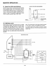
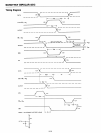
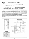
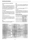
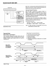
PIN
CONFIGURATION
8255 BLOCK
DIAGRAM
./'--""_
,
1/0
1'\......--.-
/
PBrPBo
I/~-~
1'0
1'\......--.-
.... /
PC3·PCO
1'0
1'\.....-----./
PCrPC4
S~~~lEI~S
1--
+SV
--GND
1'0
1'\.,....---./
PA7·PAO
Ao---I
cs------'
iffi 0
WR
---0
:~~~~
A, I
C~~~~~L
RESET---I
BI·DIRECTIONAl
DATA
BUS
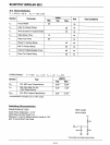
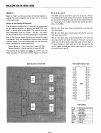
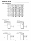
PIN NAMES
PA3
1
PA2 2
39
PA5
PAl
3
38
PA6
PAO
4
37
PA7
AD
5
36
WR
cs
G
35
RESET
GNO
7
34
DO
Al
8
33
0
1
AO
9
32
O
2
PC7
10
31
0
3
PCG
11
8255
30
0
4
PC5
12
29
Os
PC4
13
28
0
6
PCO
14
27
~
PCl
15
26
V
CC
PC2
16
25
PB7
PC3 17
24
PB6
PBO
18
23
PB5
PB1
19
22
PB4
PB2
20
21
PB3
0
7
-0
0
DATA
BUS
(BI-DIRECTIONAL)
RESET RESET INPUT
CS
CHIP SELECT
RD
READ
INPUT
WR
WRITE
INPUT
AO,A1 PORT ADDRESS
PA7·PAO.
PORT A
(BIT)
PB7·PBO
PORT B
(BIT)
PC7·PCO
PORT C
(BIT)
VCC
+5
VOLTS
GND
gVOLTS
5-113