


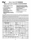

intel®
. Silicon Gate MOS
M8080A
SINGLE CHIP 8-BIT N-CHANNEL MICROPROCESSOR
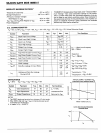
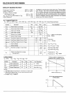
• Full Military Temperature Range
-55°C
to +125°C
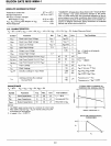
• ±10% Power Supply Tolerance
• 2
J-Ls
Instruction Cycle
• Powerful Problem Solving
Instruction Set
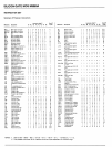
• Six General Purpose Registers
and an Accumulator
• Sixteen
Bit
Program Counter for
Directly Addressing up
to
64K Bytes
of Memory
• Sixteen Bit Stack Pointer and Stack
Manipulation Instructions for Rapid
Switching
of
the Program Environment
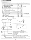
• Decimal,Binary and Double
Precision
Arithmetic
•
Ability
to Provide Priority Vectored
Interrupts
•
512
Directly Addressed
I/O
Ports
• TTL Drive Capability
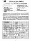
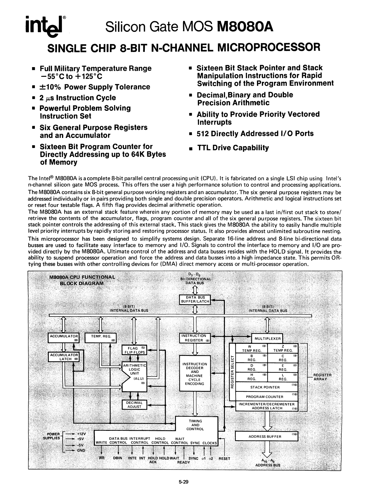
The
Intel® MaOaOA
is
a
complete
a-bit
parallel central processing
unit
(CPU). It
is
fabricated
on
a single
LSI
chip
using Intel's
n-channel silicon gate
MaS
process.
This
offers
the
user a high
performance
solution
to
control
and
processing applications.
The
MaOaOA
contains
six
a-bit
general
purpose
working registers and an
accumulator.
The
six general
purpose
registers may be
addressed individually
or
in pairs providing
both
single and
double
precision
operators.
Arithmetic
and
logical
instructions
set
or
reset
four
testable
flags. A fifth flag provides decimal
arithmetic
operation.
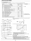
The
MaOaOA has an
external
stack
feature
wherein
any
portion
of
memory
may
be
used
as a last
in/first
out
stack
to
store/
retrieve
the
contents
of
the
accumulator,
flags, program
counter
and
all
of
the
six general
purpose
registers.
The
sixteen
bit
stack
pointer
controls
the
addressing
of
this
external stack. This
stack
gives
the
MaOaOA
the
ability
to
easily
handle
multiple
level
priority
interrupts
by rapidly storing and restoring processor status. It also provides
almost
unlimited
subroutine
nesting.
This
microprocessor has been designed
to
simplify systems design.
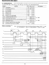
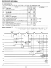
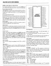
Separate
l6-line
address
and
a-line bi-directional
data
busses are used
to
facilitate easy
interface
to
memory
and I/O. Signals
to
control
the
interface
to
memory
and I/O are pro-
vided
directly
by
the
MaOaOA.
Ultimate
control
of
the
address
and
data
busses resides
with
the
HOLD signal. It provides
the
ability
to
suspend processor
operation
and
force
the
address
and
data
busses
into
a high
impedance
state.
This
permits
OR-
tying
these
busses
with
other
controlling
devices
for
(DMA)
direct
memory
access
or
mUlti-processor
operation.
5-29