


SILICON GATE MOS
8255
(RESET)
Reset: A
"high"
on this
input
clears
all
internal registers in-
cluding the Control Register and
all
ports (A,
B,
C)
are set
to
the
input mode.
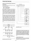
Group A and Group B Controls
The
functional configuration
of
each
port
is
programmed
by the systems software. In essence,
the
8080
CPU
"out-
puts"
a control word
to
the
8255.
The
control
word con-
tains information such as
"mode",
"bit
set",
"bit
reset"
etc.
that
initializes
the
functional configuration
of
the
8255.
Each
of
the
Control blocks (Group A and
Group
B)
accepts
"commands"
from
the
Read/Write. Control Logic, receives
"control
words"
from
the
internal
data
bus and issues
the
proper
commands
to
its associated ports.
Control
Group
A -
Port
A and Port C
upper
(C7-C4)
Control
Group
B -
Port
B and Port
Clower
(C3-CO)
The Control Word Register can
Only
be
written
into.
No
Read operation of
the
Control Word Register
is
allowed.
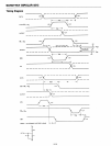
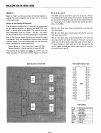
8255 BLOCK
DIAGRAM
Ports
A,
B, and C
The
8255
contains
three
8-bit
ports
(A,
S,
and C).
All
can
be configured
in
a wide variety
of
functional characteristics
by
the
system software
but
each has its own speci
al
features
or
"personality"
to
further
enhance
the
power and flexi-
bil
ity
of
the
8255.
Port A: One 8-bit
data
output
latch/buffer and one 8-bit
data
input
latch.
Port B:
One
8-bit
data
input/output
latch/buffer
and
one
8-bit
data
input
buffer.
Port
C:
One
8-bit
data
output
latch/buffer and
one
8-bit
data
input
buffer (no latch for input). This
port
can be di-
vided into
two
4-bit
ports
under
the
mode
control.
Each
4-
bit
port
contains a 4-bit latch and it can be used for
the
control signal
outputs
and
status
signal
inputs
in
conjunc-
tion with Ports A and
B.
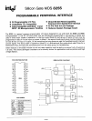
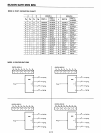
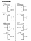
PIN CONFIGURATION
5-115
PA3
1 PA4
PA2
2
39
PA5
PAl
3
38
PA6
PAO
4
37
PA7
AD
5
36
WR
cs
6
35
RESET
GNO
7
34
DO
A1
8
33
0,
AO
9
32
O
2
PC7
10
31
0
3
PC6
11
8255
30
0
4
PC5
12
Os
PC4
13
0
6
PCO
14
0,
PC1
15
26
V
CC
PC2
16
P87
PC3
17
24
P86
P80
18
23
P85
P81
19
22
P84
P82
20
21
P83
PIN NAMES
0
7
-0
0
DATA
BUS (BI-DIRECTIONAL)
RESET
RESET INPUT
CS
CHIP SELECT
RD
READ INPUT
WR
WRITE INPUT
AO,A1
PORT ADDRESS
PA7·PAO
PORT A (BIT)
PB7·PBO
PORT B (BIT)
PC7·PCO
PORT C (SfT)
j
VCC
+5VOL1S
1
GND
"VOLTS