


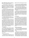

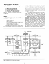
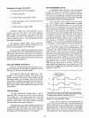
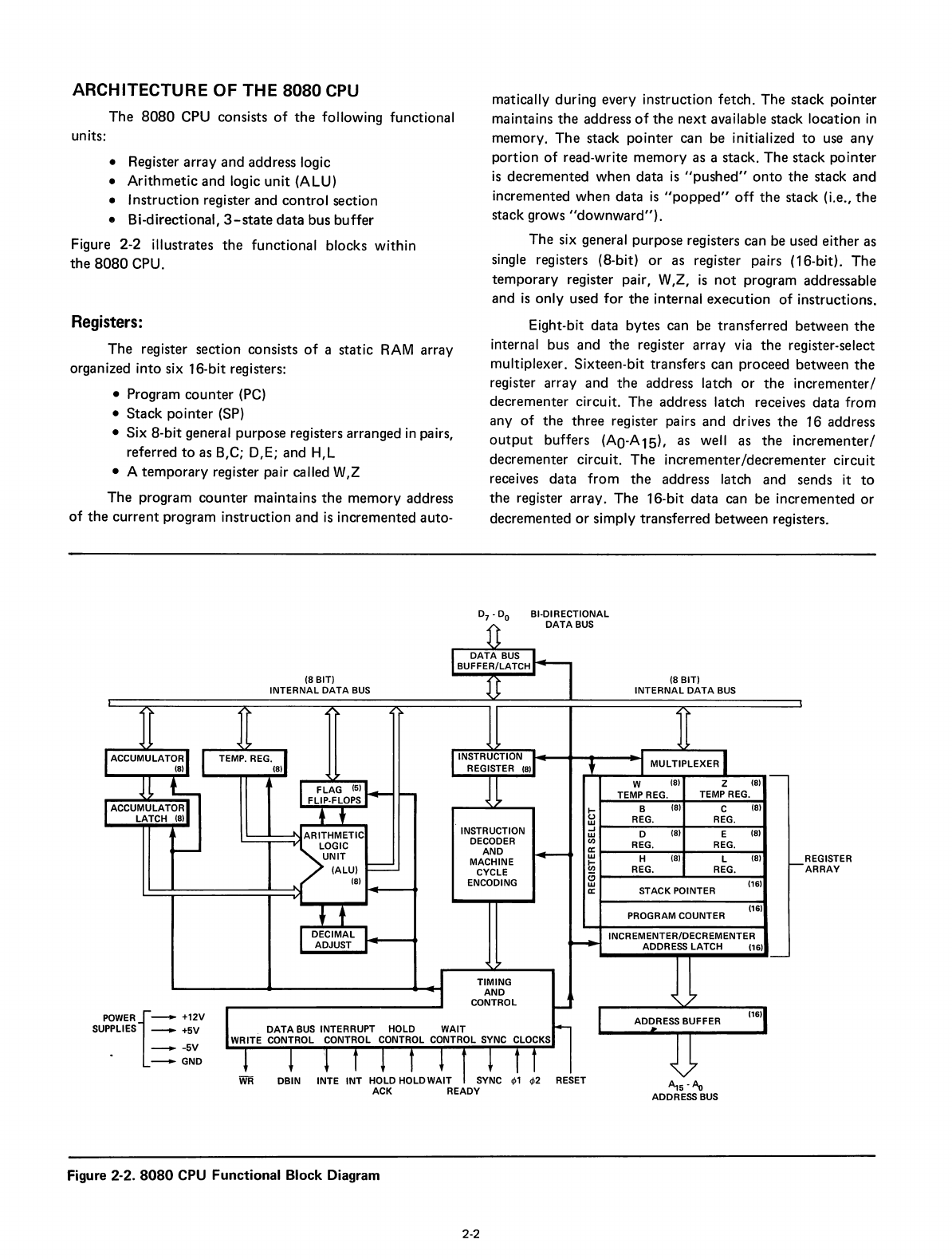
ARCHITECTURE OF THE 8080
CPU
The
8080
CPU consists
of
the
following
functional
units:
• Register
array
and
address
logic
•
Arithmetic
and
logic
unit
(ALU)
• I
nstruction
register
and
control
section
• Bi-directional,
3-state
data
bus
buffer
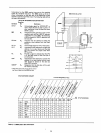
Figure
2-2
illustrates
the
functional
blocks
within
the
8080
CPU.
Registers:
The
register
section
consists
of
a
static
RAM
array
organized
into
six 16-bit registers:
• Program
counter
(PC)
•
Stack
pointer
(SP)
• Six
8-bit
general
purpose
registers arranged
in
pairs,
referred
to
as S,C; D,E;
and
H,L
• A
temporary
register pair called W,Z
The
program
counter
maintains
the
memory
address
of
the
current
program
instruction
and
is
incremented
auto-
matically during every
instruction
fetch.
The
stack
pointer
maintains
the
address
of
the
next
available stack
location
in
memory.
The
stack
pointer
can
be
initialized
to
use
any
portion
of
read-write
memory
as a
stack.
The
stack
pointer
is
decremented
when
data
is
"pushed"
onto
the
stack
and
incremented
when
data
is
"popped"
off
the
stack (Le.,
the
stack grows
"downward").
The
six general
purpose
registers
can
be used
either
as
single registers (8-bit)
or
as register pairs (16-bit).
The
temporary
register pair, W,Z,
is
not
program
addressable
and
is
only
used
for
the
internal
execution
of
instructions.
Eight-bit
data
bytes
can be
transferred
between
the
internal bus
and
the
register
array
via
the
register-select
multiplexer.
Sixteen-bit
transfers
can
proceed
between
the
register
array
and
the
address
latch
or
the
incrementer
/
decrementer
circuit.
The
address
latch receives
data
from
any
of
the
three
register pairs
and
drives
the
16
address
output
buffers
(AO-A
15), as well as
the
i
ncrementer
/
decrementer
circuit.
The
incrementer/decrementer
circuit
receives
data
from
the
address latch
and
sends it
to
the
register
array.
The
16-bit
data
can be
incremented
or
decremented
or
simply
transferred
between
registers.
81-01
RECTIONAL
DATA
BUS
A
15
-Ao
ADDRESS BUS
RESET
W
(8)
Z
(8)
TEMP REG.
TEMP REG.
B
(8)
C
(8)
...
0
REG. REG.
w
INSTRUCTION
..J
0
(8)
E
(8)
w
DECODER
en
REG. REG.
AND
a:
MACHINE
w
H
(8)
L
(8)
REGISTER
...
CYCLE
en
REG. REG.
ARRAY
ENCODING
a
(16)
w
a:
STACK POINTER
(16)
PROGRAM COUNTER
DATA
BUS
INTERRUPT HOLD
WAIT
WRITE CONTROL CONTROL CONTROL CONTROL SYNC CLOCKS
ACK
POWER
1-"
+12V
SUPPLI
ES
---.
+5V
---.
-5V
..
---.
GND
Figure 2-2.
8080
CPU
Functional Block Diagram
2-2