


intel
e
Silicon Gate CMOS 5101, 5101-3, 5101L,
5101L·3
1024
BIT
(256
x
4)
STATIC CMOS
RAM
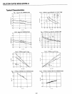
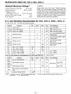
*Ultra
Low Standby Current: 15
nA/Bit
for the
5101
• Fast Access Time-
650
ns
• Single
+5
V Power Supply
•
CE
2
Controls Unconditional
Standby Mode
• Directly TTL Compatible- All
Inputs and Outputs
• Three-State Output
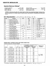
The Intel® 5101 and 5101-3 are ultra-low power 1024
bit
(256 words x 4-bits) static RAMs fabricated with an advanced ion-
implanted silicon gate CMOS technology.
The
devices have
two
chip enable inputs. When CE
2
is
at
a low level,
the
minimum
standby
current
is
drawn
by
these devices, regardless
of
any
other
input transitions
on
the
addresses and
other
control
inputs.
Also, when
CE
l
is
at
a high level and address and
other
control transitions are inhibited,
the
minimum
standby
current
is
drawn
by
these devices. When
in
standby
the
5101 and 5101-3 draw from
the
single 5
volt
supply
only
15 microamps and
200
microamps, respectively. These devices are ideally suited for low power applications where
battery
operation
or
battery
backup for non-volatility are required.
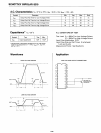
The 5101 and 5101-3 use fully DC stable (static) circuitry; it
is
not
necessary
to
pulse
chip
select for each address transition.
The data
is
read
out
non-destructively and has
the
same polarity
as
the
input
data. All inputs and
outputs
are directly
TTL
compatible.
The
5101 and 5101-3 have separate
data
input
and data
output
terminals.
Art
output
disable function
is
provided
so
that
the
data
inputs and
outputs
may be wire OR-ed for use
in
common
data
I/O systems.
The
5101
Land
5101
L-3
are identical to the 5101 and 5101-3, respectively,
with
the additional feature
of
guaranteed data
retention
at
a power supply voltage
as
low
as
2.0
volts.
A pin compatible N-channel static RAM,
the
Intel
2101,
is
also available
for
low
cost
applications where a
256
x 4 organi-
zation
is
needed.
The Intel ion-implanted, silicon gate,
complementary
MOS
(CMOS) allows
the
design and
production
of
ultra-low power,
high performance memories.
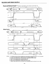
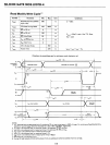
DO,
@ V
~ec
~GNO
o=
PIN
NUMBERS
CELL ARRAY
32 ROWS
32
COLUMNS
ROW
DECODERS
BLOCK
DIAGRAM
@
00
011
-01
4
DATA
INPUT
00
OUTPUT
DISABLE
Ao-A.,
ADDRESS
INPUTS
00,-
00
4
OAT
A OUTPUT
RIW
READIWRITE
INPUT
Vee.
POWER
(+5VI
ffi,CE2
CHIP
ENABLE
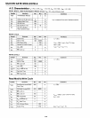
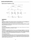
PIN CONFIGURATION LOGIC SYMBOL
5101
5101
A
3
22
Vee
Ao
A
2
2
21
A
4
A,
A,
3
20
RIW
A
2
Ao
4
19
CE1
A
3
A
4
As
5
18
00
As
~
6
17
CE2
~
A
7
A
7
7
16
00
4
GNO
8
15
01
4
01, DO,
01
2
00
2
01,
9
14
00
3
01
3
00
3
DO,
10
13
01
3
01
4
00
4
00
01
2
11
12
00
2
RIW
CE2
CE1
PIN NAMES
5-91