


SILICON GATE
MOS
M8080A
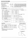
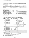
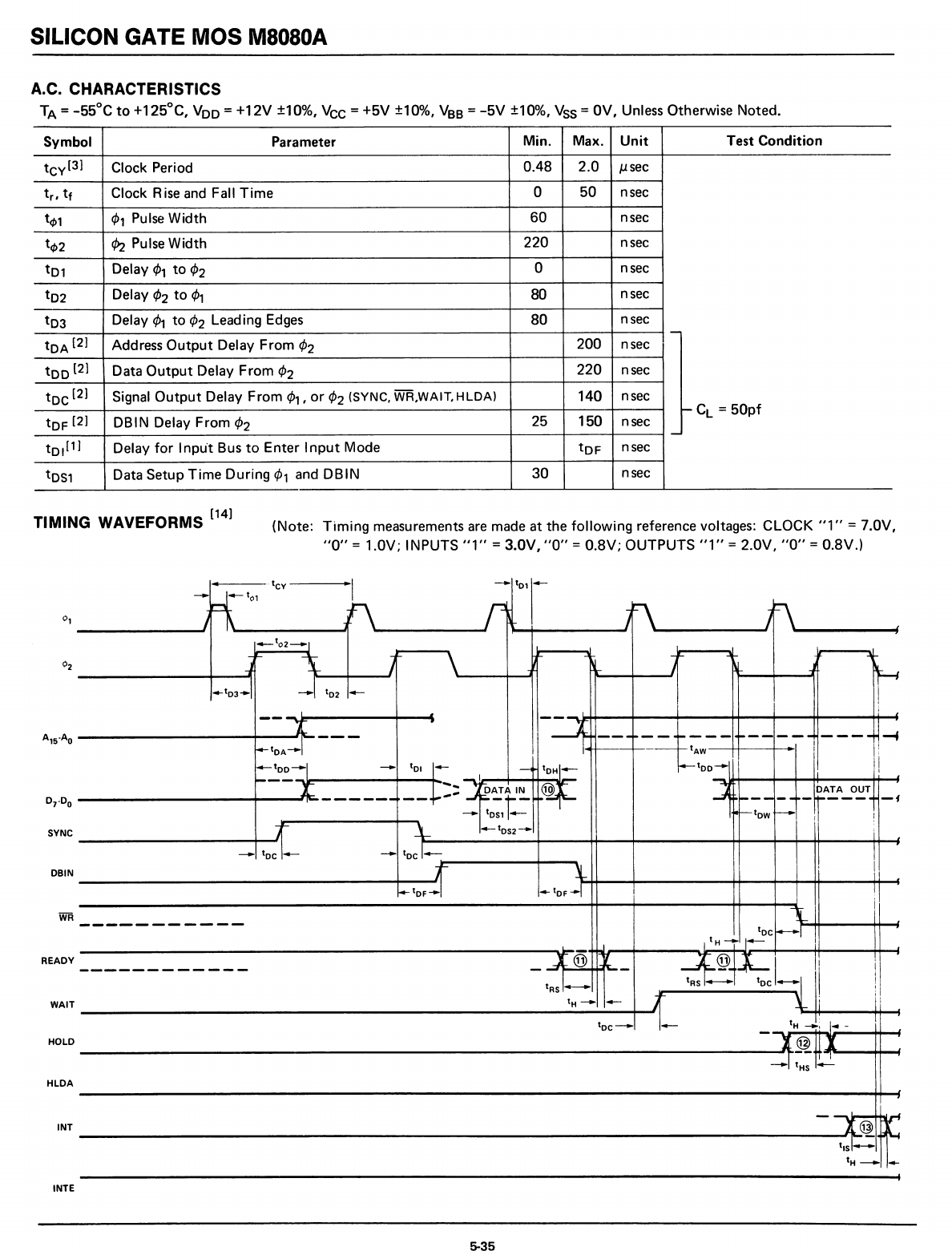
A.C. CHARACTERISTICS
TA
=
-55°C
to
+125°C,
Voo
=
+12V
±10%, Vee =
+5V
±10%,
VBB
=
-5V
±10%,
Vss
= OV, Unless Otherwise Noted.
Symbol
Parameter
Min. Max.
Unit
Test Condition
tCy[3]
Clock Period
0.48 2.0
Jisec
t
r
,
tf
Clock Rise
and
Fall
Time
0
50
nsec
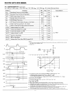
t(/>l
epl
Pulse
Width
60 nsec
tep2
cI>2
Pulse
Width
220 nsec
t01
Delay
epl
to
4>2
0
nsec
t02
Delay
~2
to
~1
80
nsec
t03
Delay
~1
to
~2
Leading
Edges
80
nsec
-
tOA
[2)
Address
Output
Delay From
~2
200 nsec
too
[2]
Data
Output
Delay From
~2
220 nsec
toc
[2]
Signal
Output
Delay From
~1,
or
~2
(SYNC,
WR,WAIT,HLDA)
140
nsec
tOF
[2]
DBIN Delay From
ep2
25 150
- C
L
=
50pf
nsec
-
tOI[l)
Delay
for
Input
Bus
to
Enter
Input
Mode
tOF
nsec
tOSl
Data Setup
Time
During
~1
and
DBIN
30
nsec
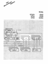
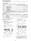
TIMING WAVEFORMS
[14]
(Note:
Timing
measurements
are
made at the
following
reference voltages: CLOCK
"1"
=7.0V,
"0"
= 1.0V; INPUTS
"1"
=
3.0V,
"0"
=
0.8V;
OUTPUTS
"1"
= 2.0V,
"0"
= 0.8V.)
SYNC
DBIN
READY
WAIT
HOLD
HLDA
INT
INTE
..
·t
ey
-\
--.
1
01
1-
--.
F\I
01
I
f\
r~
t\
Jf\
...-t
o2
-"
1
....,~
7~
~~
~
I~
~
r-
..,
-J
~
.....
~
r
....
t
o3
.....!
--.1
t
02
.--
.
I
--x
.
-=1
~~
-
---
--
~---
~--
---
----
...-t
OA
-'!
--
~tAW
.--too--'I
-.
to!
1'-
--t
t
oH
I4--
f.--t
OO
-'
i
I
...
r
_I
)
__
+:=:
J~~A
I~
~
DATA
OUT
------
-
'osl1=-1
~--
--
-
-----
-f
..
~tow
~
i
!
T
-\-
..-
t
OS2
-'
i
-.
t
oc
14-
--.
tocl..-
I
~
t
I
~toF-.1
....
toF~1
!
~t
I
-~~--------
t
oc
~I
L
,tHil'-
------------
~@
r
-
&~~I
I
I
--
IRS""':'
loe
-I
I
tRsl~
t
H
--.
.--
1-
li
t
oc
-"'"
_ t
H
-.;
1·-
I@
I~
--.r~;I~
-I~
[I-
~~
tH~
....
5-35