


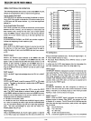
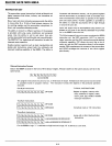
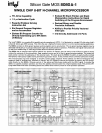
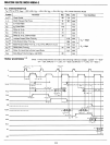
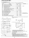

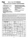
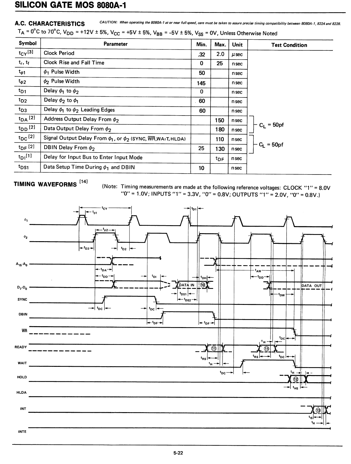
SILICON GATE MOS 8080A-1
A.
c.
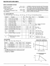
CHARACTERISTI
CS
CA
UTlON:
When
operating the
8080A·l
at
or
near
full
speed,
care
must
be
taken to
assure
precise timingcompatibilitybetween
8080A·',
8224and 8228.
TA =
O°C
to
70°C,
Voo
=
+12V
± 5%,
VCC
=
+5V
±
5%,
VSS
=
-5V
±
5%,
VSS
=OV, Unless Otherwise Noted
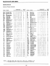
Symbol
Parameter
Min. Max. Unit
Test Condition
tCy[3]
Clock Period
.32
2.0
J.1sec
t
r
,
tf
Clock Rise and Fall
Time
0
25
nsec
t4»1
¢1
Pulse
Width
50
nsec
t4»2
~
Pulse
Width
145
nsec
t01
Delay
cfJ1
to
cfJ2
0
nsec
t02
Delay ¢2
to
cfJ1
60
nsec
t03
Delay ¢,
to
¢2 Leading
Edges
60
nsec
tOA [2]
Address
Output
Delay From ¢2
150
nsec
}
Cl
= 50pf
too
[2]
Data
Output
Delay From ¢2
180
nsec
toc[2]
Signal
Output
Delay From
¢"
or
cfJ2
(SYNC,
WR.WAIT,
HLOA)
110
nsec
}C
l
=50pf
tOF
[2]
DBIN
Delay
From
¢2
25
130
nsec
tOI[1]
Delay
for
Input
Bus
to
Enter
Input
Mode
tOF
nsec
tOS1
Data Setup
Time
During
cfJ1
and
DBIN
10
nsec
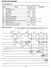
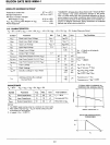
TIMING WAVEFORMS [14]
(Note:
Timing
measurements
are
made at the
following
reference voltages:
CLOCK
111"
=
8.0V
110"
=
1.0V;
INPUTS
111"
=
3.3V,
1'0" =
0.8V;
OUTPUTS
"1"
=
2.0V,
"0"
= O.8V.)
SYNC
DBIN
READY
WAIT
HOLD
HLDA
INT
INTE
.
t
CY
~I
---.
~11-
---.
Fft~l
I
f\
r~
Jf\
}F\
~t~2~1
-~
}~
1~~
~
-~
..Jjl-
.....,J-
1
-J
~k-
I
~
"1
~
...
t
03
"'!
-.\
t
02
~
--~
.
-=1
.
i4--
t
OA-'\
-
---
1---
~---
---
---
----
--f
I
tAW
i4---too~1
-...
t
OI
1'-
--t
toHI'-
~tOO-"
~
r
-
~
.J
+:
.....
H"
DATA
OUT
.,._
.JrPATA
IN
,-
--
~-t-
1---
-- -
10----
-I
-...
t
OS1
...-
I-f--t
ow
~
T
-i-
.....
t
oS2
.....
---.
toc
1.-.
.-.
tocl.-
-r
t
~tOF:.I
...
t
OF
-----------
~l
t
oc
.-.-.\
L-,
I t
H
-ij
r--
--_
....
_------~-
-r@
t
~~
I
-tRSI-
'RS
toe
-'-{
I
t
H
-.
.-
T
I~
I
t
oc
---'
_ t
H
-.1
1.-
!@
IX
~r~:~
-
L
!@
~
tiS
1==
~~
t
H
-...
...
5-22