


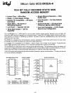

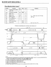
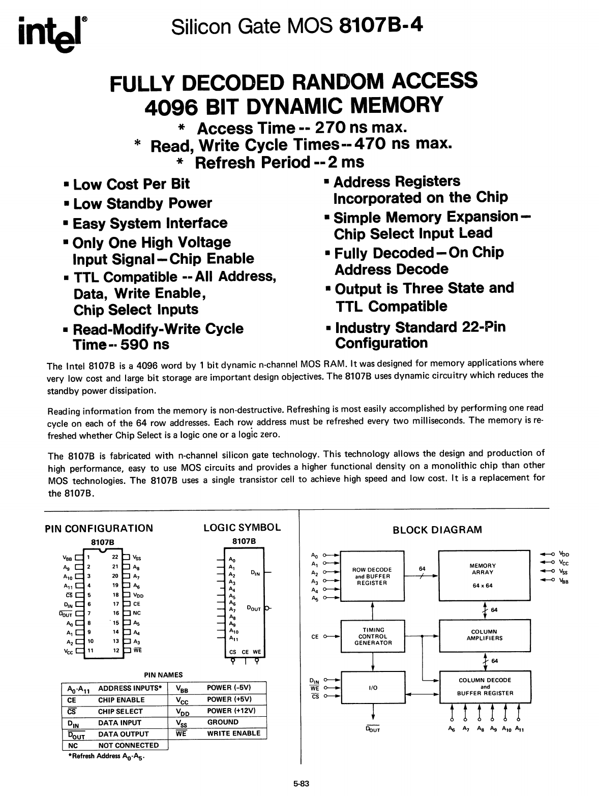
Silicon Gate MOS
81078·4
FULLY
DECODED RANDOM ACCESS
4096
BIT
DYNAMIC MEMORY
* Access
Time··
270
ns max.
* Read, Write Cycle
Times--470
ns max.
* Refresh Period -- 2 ms
• Low Cost Per Bit • Address Registers
• Low Standby Power Incorporated on the Chip
• Easy System Interface • Simple Memory
Expansion-
• Only One High Voltage Chip Select Input Lead
Input
Signal-
Chip Enable • Fully Decoded - On Chip
•
TTL
Compatible -- All Address, Address Decode
Data,
Write Enable, • Output is Three State and
Chip Select Inputs TTL Compatible
• Read-Modify-Write Cycle • Industry Standard 22-Pin
Time
_.
590
ns Configuration
The Intel
81078
is
a
4096
word
by 1
bit
dynamic
n-channel
MOS
RAM. It was designed
for
memory
applications
where
very low
cost
and large
bit
storage are
important
design objectives.
The
81078
uses
dynamic
circuitry which reduces
the
standby
power dissipation.
Reading information from
the
memory
is
non-destructive. Refreshing
is
most
easily accomplished
by
performing
one
read
cycle
on
each
of
the
64
row addresses. Each row address must be refreshed every
two
milliseconds.
The
memory
is
re-
freshed
whether
Chip Select
is
a logic
one
or
a logic zero.
The
81078
is
fabricated
with
n-channel silicon gate technology. This technology allows
the
design and
production
of
high performance, easy
to
use
MOS
circuits and provides a higher functional density on a
monolithic
chip
than
other
MOS
technologies.
The
81078
uses a single transistor cell
to
achieve high speed and low cost.
It
is
a replacement for
the
81078.
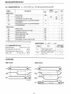
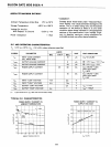
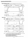
Ao-A"
ADDRESS INPUTS*
V
BB
POWER (-5V)
CE
CHIP
ENABLE
Vee
POWER (+5V)
CS
CHIP SELECT
V
OO
POWER
(+12V)
DIN
DATA
INPUT
V
ss
GROUND
D
OUT
DATA
OUTPUT
WE
WRITE
ENABLE
NC
NOT CONNECTED
PIN CONFIGURATION
81078
Vee
V
ss
Ag
As
A,o
A]
A"
~
CS
Vee
o.N
CE
DouT
NC
Ao
As
A,
A.1
A
2
A3
Vee
WE
PIN NAMES
*Refresh Address A
o
-As'
LOGIC SYMBOL
81078
Ao
A,
A
2
DIN
A
J
A
4
As
A
6
A]
D
OUT
As
Ag
A,o
A"
CS CE
WE
5-83
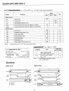
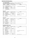
BLOCK
DIAGRAM
A
O
0----.
.......0
"be
A,
0----.
MEMORY
~
Vee
ROW DECODE
64
A
2
and
BUFFER
ARRAY
~
V
ss
A
J
0----.
REGISTER
.......0
"BB
A
4
64
x
64
~
0----.
f64
TIMING
COLUMN
CE
0----.
CONTROL
AMPLIFIERS
GENERATOR
64
DIN
0----.
WE
0----.
I/O
CS
0----.