


Silicon Gate MOS 8251
PROGRAMMABLE COMMUNICATION INTERFACE
..
Synchronous and Asynchronous
Operation
• Synchronous:
5-8 Bit Characters
Internal
or
External Character
Synchronization
Automatic
Sy.nc
Insertion
• Asynchronous:
5-8
Bit Characters
Clock Rate
-1,16
or
64 Times
Baud Rate
Break Character Generation
1,
1
1
h,
or
2 Stop Bits
False Start Bit Detection
• Baud Rate - DC
to
56
k
Baud
(
Sync
Mode)
DC
t09.6k
Baud
(Async
Mode)
• Full Duplex,
Double
Buffered,
Transmitter
and Receiver
•
Error
Detection
- Parity, Overrun,
and Framing
• Fully
Compatible
with
8080 CPU
• 28-Pin DIP
Package
•
All
Inputs and
Outputs
Are
TTL
Compatible
•
Single
5
Volt
Supply
•
Single
TTL
Clock
The 8251
is
a Universal Synchronous/Asynchronous Receiver / Transmitter(USA
RT)
Chip designed for data
communications
in
microcomputer systems. The USART
is
used
as
a peripheral device and
is
programmed
by
the
CPU
to
operate using virtually any serial data transmission technique presently
in
use (including
IBM
Bi-Sync). The USART accepts data characters from the
CPU
in
parallel format and then converts them into
a continuous serial data stream for transmission. Simultaneously it can receive serial data streams and con-
vert them into. parallel data characters for
the
CPU.
The USART will signal the
CPU
whenever it can accept
a
new
character for transmission
or
whenever it has received a character for the CPU. The
CPU
can read the
complete status of
the
USART
at
any time. These include data transmission errors and control signals such
as
SYNDET, TxEMPT. The chip
is
constructed using N-channel silicon gate technology.
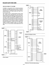
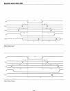
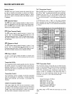
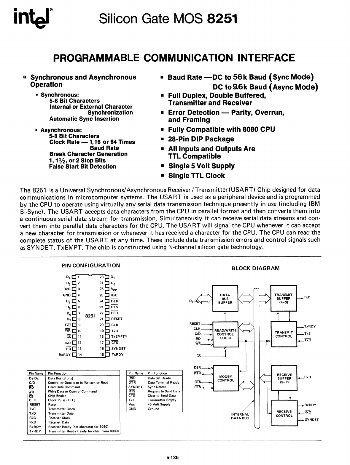
RxRDY
RxC
RxD
TxD
.....
SYNDET
TxRDY
TRANSMIT
TxE
CONTROL
TRANSMIT
BUFFER
(p
....
S)
BLOCK
DIAGRAM
/
INTERNAL
DATA
BUS
Pin
Name
Pin
Function
DSR
Data
Set
Ready
DTR
Data Terminal Ready
SYNDET
Sync Detect
RTS Request to
Send
Data
CTS
Clear
to
Send
Data
TxE Transmitter Empty
Vee
+5
Volt
Supply
GND Ground
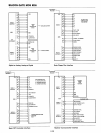
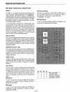
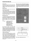
PIN
CONFIGURATION
O
2
0
1
0
3
Do
RxD
Vee
GND
RxC
0
4
DTR
0
7
-0
0
05
RTS
0
6
DSR
0
7
RESET
fXC
CLK
WR
TxD
CS
TxEMPTY
C/O
CTS
RD
SYNDET
RxRDY
TxRDY
Pin
Name
Pin
Function
07-
0
0
Data
Bus
(8 bits)
C/O Control
or
Data
is
to
be Written or
Read
AD
Read
Data Command
WR
Write Data orControl Command
Cs
Chip Enable
CLK Clock
Pulse
(TTL)
RESET
Reset
TxC Transmitter Clock
TxD
Transmitter Data
RxC
Receiver Clock
RxD
Receiver
Data
RxRDY
Receiver Ready
(has
character for 8080)
TxRDY
Transmitter Ready (ready
for
char. from 8080)
5-135