


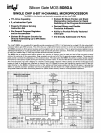
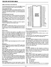


SILICON GATE MOS
8080A-1
ABSOLUTE MAXIMUM
RATINGS·
Temperature Under Bias
O°C
to
+70° C
Storage Temperature
-65°C
to
+150°C
All
I
nput
or
Output
Voltages
With Respect
to
Vaa
-0.3V
to
+20V
Vee,
VOO
and Vss With Respect
to
Vaa
-0.3V
to
+20V
Power Dissipation . . . . . . . . . . .
..
1.5W
*COMMENT: Stressesabove those listedunder
'Absolute
Maxi-
mum
Ratings"
may
cause
permanent damage
to
the device.
This is a stress rating
only
and
functional
operation
of
the
de-
vice
at
these
or
any
other
conditions
above those indicated
in
the operational sections
of
this specification
is'not
implied. Ex-
posure
to
absolute
maximum
rating conditions
for
extended
periods
may
affect
device reliability.
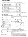
D.C. CHARACTERISTICS
TA
=
O°C
to
70°C,
Voo
=
+12V
± 5%,
Vce
=
+5V
±
5%,
Vss
=
-5V
±
5%,
Vss =OV, Unless Otherwise Noted.
Symbol
Parameter
Min.
Typ.
Max.
Unit
Test
Condition
VILe
Clock
Input
Low
Voltage
Vss-1
Vss+0.8
V
VIHC
Clock
Input
High Voltage
9.0
Voo+1
V
VIL
Input
Low
Voltage
Vss-1
Vss+0.8
V
VIH
Input
High Voltage
3.3
Vec+1
V
VOL
Output
Low
Voltage 0.45 V
}
'0
L =
1.9mA
on
all outputs,
VO
H
Output
High Voltage 3.7
V
'OH
=
150J,.lA.
1
00
(AV)
Avg. Power
Supply
Current
(Voo)
40
70
mA
ICC
(AV)
Avg. Power Supply Current
(Vce)
60
80
mA
} Operation
T
Cy
= .32Jlsec
'ss
(AV)
Avg. Power
Supply
Current
(V
ss
)
.01
1
mA
IlL
Input
Leakage ±10
pA
Vss
~
VIN
~
Vee
ICl
Clock Leakage
±10
pA
Vss
~
VeLOeK
~
V
oo
IOL[2]
Data Bus Leakage in
Input
Mode
-100
JlA
VSS~VIN
~Vss+0.8V
-2.0
mA
Vss+0.8V~VIN
~Vec
IFL
Address and Data Bus Leakage
+10
pA
VAOOR/OATA =
Vec
During
HOLD
-100
VAOOR/OATA =
VSS
+
0.45V
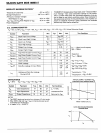
+75
+25
+50
0.5
----"'-----....L..-
....J
o
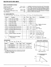
TYPICAL
SUPPLY
CURRENT
VS.
TEMPERATURE,
NORMALIZED.[3]
AMBIENT TEMPERATURE
(OC)
1.5
r------r-----~---_
~
z
w
a:
a:
::>
(J
1.0
1"-----=-~:------+-------4
>
-'
Q.
Q.
::>
en
Symbol
Parameter
Typ.
Max.
Unit
Test Condition
Cf/>
Clock Capacitance
17
25
pf
f
c
= 1
MHz
CIN
I
nput
Capacitance
6
10
pf
Unmeasured Pins
CO
UT
Output
Capacitance
10
20
pf
Returned
to
VSS
NOTES:
1.
The
RESET
signal
must
be
active for a minimum of 3 clock
cycles.
2.
When
OSIN
is
high
and
VIN
>
VIH
an
internal
active
pull
up
will
be
switched
onto
the
Data
Sus.
3.
aI
supply
I b.TA =
-0.45%/
c.
CAPACITANCE
T
A
= 25°C Vee =
VOO
= Vss = OV,
Vas
=-5V
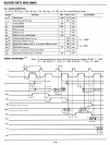
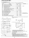
DATA
BUS CHARACTERISTIC
DURING
DBIN
MAX
°o'-------------~
Vee
5-21