SCHOTTKY BIPOLAR
8210
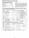
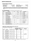
Absolute Maximum Ratings*
Temperature Under
Bias
o°c
to
70°C
Storage Temperature
-65°C
to
+150°C
Supply Voltage, Vee
-0.5
to
+7V
Supply Voltage, V
oo
-0.5
to
+13V
All
Input
Voltages
-1.0
to
+5.5V
Outputs
for
Low
Voltage Drivers . . . . . .
..
-0.5
to
+7V
Outputs
for
Clock Driver
-1.0
to
+13V
Power Dissipation at 25°C
2W
*COMMENT: Stresses above
those
listed under "Absolute Maximum Ratings" may cause
permanent
damage
to
the
device. This.is a
stress rating only and functional operation
of
the
device
at
these or any
other
conditions above those indicated in
the
operational sec-
tions of this specification
is
not
implied. Exposure
to
absolute maximum rating conditions for
extended
periods may affect device
reliability.
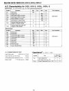
D.C.
Characteristics
TA
=
O°C
to
70°C,
VCC
=
5.QV
±
5%,
VDD
=12V ±
5%
Symbol
Parameter
Min.
Max.
Unit
Test Conditions.
'FO
Data Input Load Current
-0.25
mA
VF
= 0.45V
IFE
Enable I
nput
Load Current
-0.50
mA
VF
= 0.45V
I
RO
Data
.1
nput
Leakage
Current
10
p.A
V
R
= 12.6V
IRE
Enable
Input
Leakage
Current
20
p.A
V
R
= 12.6V
VOL
Output
Low Voltage
0.45 V
IOl
=
3mA,
V1H
= 2V
for
all Drivers
-1.0
V
IOl
=
-5mA
VO
H1
Output
High Voltage
Vee
-1.0
V
IOH
=
-1
mA,
V
il
= 0.8V
for
Low Voltage 0rivers
V
CC
+1.0 V
'OH
=
5mA
VOH2
Output
High Voltage
V
OO
-0.75
V
IOH
=
-1
mA,
Vll
= 0.8V
for
High Voltage Driver
VOO
+ 0.5
V
IOH
=
5mA
101
Pulsed
Output
Sink Current
75
mA
Vo =
2V,
VI
H=
2V
for
Low Voltage Drivers
102
Pulsed
Output
Sink Current
100
mA
VO=3V,
VIH
=2V
for
High Voltage Driver
1
03
Pulsed
Output
Source Current
-75
mA
Vo =
VCC
-1.5V,
for
Low
Voltage Drivers
VIL = O.8V
1
04
Pulsed
Output
Source Current
-100
mA
Va = Voo
-3V,
for
High Voltage Driver
VIL = 0.8V
VIL
Input
Low Voltage,
All
Inputs
0.8 V
VIH
Input
High Voltage,
All
Inputs
2
V
POWER
SUPPLY CURRENT
DRAIN
AND
POWER
DISSIPATION
All
driver
outputs
are
in
the
state
indicated
Test Conditions -- I
nput
states
to
ensu
re
the following
output
states:
Additional Test
Symbol
Parameter
Typ.l1]
Max.
Unit
All
Low Voltage
High Voltage
Conditions
Outputs
Output
leCl
Cu
rrent from Vce
26
35
mA
Low
Low
1001
Current from Voo
12
16
mA
Low
Low
POl
Power Dissipation
290
390
mW
Low
Low
ICC2
Cu
rrent from Vcc
21
28 'mA
Low High
1002
Current from Voo
26
35
mA
Low High
P02
Power 0 issipation 450 600
mW
Low
High
V
CC
=5.25V,
leC3
Current from Vec
19 25
mA
High
Low
V
oo
= 12.6V
1003
Current from Voo
12
16
mA
High
Low
P03
Power 0 issipation
260
340
mW
High
Low
ICC4
Cu
rrent from Vce
14
18
mA
High
High
1004
Current
from
Vo
o
26
35
mA
High
High
PD4
Power 0 issipation
410 550
mW
High
High
[l]This
parameter
is
periodically sampled
and
is
not
100% tested. Condition of measurement
is
TA =25°C,
VCC
= 5V,
VOO
= 12V.
5-97


