


While
no
one
instruction
cycle will
consist
of
more
then
five
machine
cycles,
the
following
ten
different
types
of
machine cycles
may
occur
within
an
instruction
cycle:
(1
)
FETCH (M1)
(2)
MEMORY READ
(3)
MEMORYWRITE
(4)
STACK
REAO
(5)
STACK
WRITE
(6)
INPUT
(7)
OUTPUT
(8)
INTERRUPT
(9)
HALT
(10)
HALT.
INTERRUPT
The
machine
cycles
that
actually
do
occur
in
a par-
ticular
instruction
cycle
depend
upon
the
kind
of
instruc-
tion,
with
the
overriding
stipulation
that
the
first
machine
cycle in
any
instruction
cycle
is
always
a
FETCH.
The
processor identifies
the
machine
cycle
in
prog-
ress
by
transmitting
an
eight-bit
status
word
during
the
first
state
of
every
machine
cycle.
Updated
status
information
is
presented
on
the
8080's
data
lines
(00-07),
during
the
SYNC interval.
This
data
should
be saved in latches,
and
used
to
develop
control
signals
for
external
circuitry.
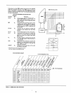
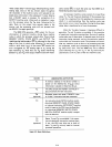
Table
2-1 shows
how
the
positive-true
status
information
is
dis-
tributed
on
the
processor's
data
bus.
Status
signals are
provided
principally
for
the
control
of
external
circuitry.
Simplicity
of
interface,
rather
than
machine cycle
identification,
dictates
the
logical
definition
of
individual
status
bits.
You
will
therefore
observe
that
certain processor
machine
cycles are
uniquely
identified
by
a single
status
bit,
but
that
others
are
not.
The
M1
status
bit
(06),
for
example,
unambiguously
identifies
a FETCH
machine cycle. A STACK
REAO,
on
the
other
hand,
is
indicated
by
the
coincidence
of
STACK
and
MEMR
sig-
nals. Machine cycle
identification
data
is
also valuable
in
the
test
and
de-bugging phases
of
system
development.
Table
2-1
lists
the
status
bit
outputs
for
each
type
of
machine cycle.
State Transition Sequence:
Every
machine
cycle
within
an
instruction
cycle
con-
sists
of
three
to
five active
states
(referred
to
as T 1, T2, T3,
T4,
T5
or
TW).
The
actual
number
of
states
depends
upon
the
instruction
being
executed,
and
on
the
particular
ma-
chine cycle
within
the
greater
instruction
cycle.
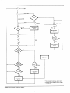
The
state
transition
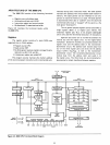
diagram in Figure 2-4
shows
how
the
8080
pro-
ceeds
from
state
to
state
in
the
course
of
a
machine
cycle.
The
diagram also
shows
how
the
READY,
HOLD,
and
INTERRUPT
lines
are
sampled
during
the
machine
cycle,
and
how
the
conditions
on
these
lines
may
modify
the
2-5
basic
transition
sequence.
In
the
present
discussion,
we
are
concerned
only
with
the
basic sequence
and
with
the
READY
function.
The
HOLD
and
INTERRUPT
functions
will be discussed later.
The
8080
CPU
does
not
directly
indicate
its internal
state
by
transmitting
a"state
contro'"
output
during
each
state;
instead,
the
8080
supplies
direct
control
output
(INTE, HLOA, OBIN, WR
and
WAIT)
for
use
by
external
circuitry.
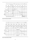
Recall
that
the
8080
passes
through
at
least
three
states
in every
machine
cycle,
with
each
state
defined
by
successive low-to-high
transitions
of
the
¢1
clock.
Figure
2-5 shows
the
timing
relationships
in
a
typical
FETCH
machine
cycle. Events
that
occur
in
each
state
are referenced
to
transitions
of
the
¢1
and
¢2
clock
pulses.
The
SYNC signal
identifies
the
first
state
(T1)
in
every
machine
cycle.
As
shown
in Figure
2-5,
the
SYNC
signal
is
related
to
the
leading
edge
of
the
¢2
clock.
There
is
a
delay
(tOC)
between
the
low-to-high
transition
of
¢2
and
the
positive-going edge
of
the
SYNC
pulse.
There
also
is
a
corresponding
delay
(also
tOC)
between
the
next
¢2
pulse
and
the
falling edge
of
the
SYNC signal.
Status
information
is
displayed
on
00-D7
during
the
same
cP2
to
cP2
interval.
Switching
of
the
status
signals
is
likewise
controlled
by
<1>2.
The
rising edge
of
¢2
during
T 1 also loads
the
pro-
cessor's
address
lines
(AO-A
15).
These
lines
become
stable
within
a brief
delay
(tDA)
of
the
cP2
clocking pulse,
and
they
remain
stable
until
the
first
¢2
pulse
after
state
T3.
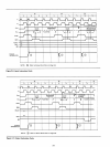
Th
is
gives
the
processor
ample
time
to
read
the
data
re-
turned
from
memory.
Once
the
processor
has
sent
an
address
to
memory,
there
is
an
opportunity
for
the
memory
to
request
a WAIT.
This it
does
by
pulling
the
processor's
READY
line low,
prior
to
the
"Ready
set-up"
interval (tRS)
which
occurs
during
the
(/)2
pulse
within
state
T2
or
TW. As long as
the
REAOY
line
remains
low,
the
processor
will idle, giving
the
memory
time
to
respond
to
the
addressed
data
request.
Refer
to
Figure 2-5.
The
processor
responds
to
a
wait
request
by
entering
an
alternative
state
(TW)
at
the
end
of
T2,
rather
than
pro-
ceeding
directly
to
the
T3
state.
Entry
into
the
TW
state
is
indicated
by
a WAIT signal
from
the
processor, acknowledg-
ing
the
memory's
request.
A low-to-high
transition
on
the
WAIT line
is
triggered
by
the
rising
edge
of
the
(/)1
clock
and
occurs
within
a
brief
delay
(tOC)
of
the
actual
entry
into
the
TW
state.
A
wait
period
may
be
of
indefinite
duration.
The
pro-
cessor remains
in
the
waiting
condition
until its
READY
line
again goes high. A
READY
indication
must
precede
the
fail-
ing edge
of
the
(/)2
clock
by
a specified interval (tRS),
in
order
to
guarantee
an
exit
from
the
TW
state.
The
cycle
may
then
proceed,
beginning
with
the
rising edge
of
the
next
(/)1
clock. A
WAIT
interval will
therefore
consist
of
an
integral
number
of
TW
states
and
will
always
be a multiple
of
the
clock
period.