


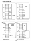

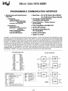
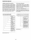

SILICON GATE MOS
8251
8251 BASIC
FUNCTIONAL
DESCRIPTION
General
The 8251
is
a Universal Synchronous!Asynchronous
Re-
ceiver/Transmitter designed specifically for
the
8080
Micro-
computer
System.
like
other
I!O devices in
the
8080
Micro-
computer
System its functional configuration
is
programmed
by
the
systems software
for
maximum flexibility.
The
8251
can
support
virtually any serial
data
technique currently
in
use (including
IBM
"bi-sync").
In
a communication environment an interface device must
convert parallel
format
system
data
into serial format for
transmission and convert incoming serial
format
data
into
parallel system
data
for reception.
The
interface device must
also delete
or
insert bits
or
characters
that
are functionally
unique
to
the
communication technique.
In
essence,
the
interface should appear
"transparent"
to
the
CPU, a simple
input
or
output
of
byte-oriented system data.
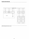
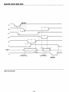
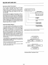
Data
Bus
Buffer
This
3-state,
bi-directional,8-bit buffer
is
used
to
interface
the
8251
to
the
8080
system Data Bus. Data
is
transmitted
or
received
by
the
buffer
upon
execution
of
INput
or
OUT-
put
instructions
of
the
8080
CPU. Control words, Command
words and
Status
information are also transferred through
the
Data Bus Buffer.
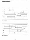
ReadlWrite Control
logic
This functional block accepts inputs from
the
8080
Control
bus and generates control signals
for
overall device operation.
It contains
the
Control Word Register and Command Word
Register
that
store
the
various control formats for device
functional definition.
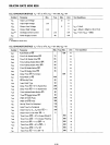
RESET (Reset)
A
"high"
on
this
input
forces
the
8251 into an
"Idie"
mode.
The device will remain
at
"Idle"
until a new
set
of
control
words
is
written into
the
8251
to
program its functional
definition.
ClK
(Clock)
C/D (Control/Data)
This input,
in
conjunction
with
the
WR
and
RD
inputs
in-
forms
the
8251
that
the
word
on
the
Data Bus
is
either
a
data
character, control word
or
status
information.
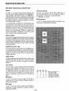
1
=CONTROL 0 =DATA
CS
(Chip Select)
A
"low"
on
this
input
enables
the
8251.
No reading
or
writ-
ing
will
occur
unless
the
device
is
selected.
The
ClK
input
is
used
to
generate internal device timing
and
is
normally connected
to
the
Phase 2 (TTL)
output
of
the
8224
Clock Generator. No external inputs
or
outputs
are referenced
to
ClK
but
the
frequency
of
ClK
must be
greater
than
30
times
the
Receiver
or
Transmitter clock
in-
puts for synchronous mode (4.5 times for asynchronous
mode).
WR
(Write)
A
"Iow"
on
this
input
informs
the
8251
that
the
CPU
is
outputting
data
or
control words,
in
essence,
the
CPU
is
writi
ng
out
to
the
8251.
RD (Read)
A
"Iow"
on
this
input
informs
the
8251
that
the
CPU
is
in-
putting
data
or
status information,
in
essence,
the
CPU
is
reading from
the
8251.
5-136
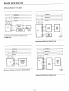
c/o
RD
WR
CS
o 0 1 0
o 1 0 0
1 0 1 0
1 1 0 0
X X X 1
8251
=>
DATA
BUS
DATA
BUS
=>
8251
STATUS=>
DATA
BUS
DATA
BUS=>
CONTROL
DATA
BUS=> 3-STATE