


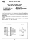
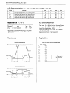
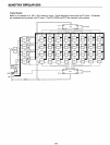


SILICON
GATE
CMOS 5101,5101-3, 5101L, 5101L-3
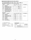
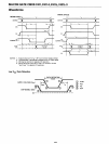
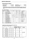
A.C.
Characteristics
for
5101, 5101· 3,
5101
L,
5101
L-
3
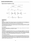
READ CYCLE TA =
o°c
to
70°C,
Vcc
=
5V
±5%, unless
otherwise
specified.
Symbol
Parameter
Min.
Typ.
Max. Unit
Test Conditions
tAC
Read Cycle
650
ns
tA
Access
Time
650
ns
teol
Chip Enable (CE1)
to
Output
600
ns
Chip Enable (CE2)
to
Output
700
(See below)
teo2
ns
too
Output
Disable
To
Output
350
ns
tOF
Data
Output
to
High Z
State
0
150
ns
tOH1'
Previous Read
Data
Valid
with
0
Respect
to
Address Change
ns
tOH2
Previous Read
Data
Valid
with
0
Respect
to
Chip
Enable
ns
WRITE CYCLE
Symbol
Parameter Min.
Typ.
Max. Unit
Test Conditions
twe
Write Cycle
650
ns
tAW
Write Delay
150
ns
tewl
Chip Enable (CE1)
To
Write
550
ns
(See below)
tCW2
Chip Enable (CE2)
To
Write
550
ns
tow
Data
Setup
400
ns
tOH
Data Hold
100
ns
twP
Write Pulse
400
ns
tWA
Write Recovery
50
ns
tos
Output
Disable
Setup
150
ns
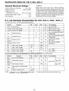
A.
C.
CONDITIONS OF TEST
C
-18
[2]
apaci nee T
A
=
25°C,
f = 1
MHz
Input
Pulse Levels: +0.65 Volt
to
2.2 Volt
Input Pulse Rise and Fall Times:
20nsec
1
TTL
Gate
and C
L
=
100pF
Timing Measurement Reference Level:
Output
Load:
1.5
Volt
Symbol
Test
Limits
(pF)
Typ.
Max.
C1N
Input
Capacitance
4
8
(All
Input
Pins) V
1N
=
OV
GoUT
Output
Capacitance
VO
UT
=
OV
8
12
5-93