


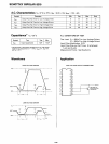


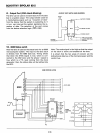

SCHOTTKY BIPOLAR
8212
OUTPUT
BUFFER
-INTERNAL
SR
FLIP-FLOP
CLR
(OS1-
0S
2)
STB
-SR
tNT
0 0
0
, ,
0
,
0
,
0
,
1
'-
0 0
,
1
0
1
0
,
0
0
1
,
1
,
~I
,
0
~D18-------~
.....
~
01
7
-------+-1-1
DATA
LATCH
ff§>
DIS
-------
..............
IE>
CLR-----001
~~_
.......
--'
(ACTIVE
LOW)
~
MO
----to4'
__
~
[jj>STB--
............
[[>012--------+-
.....
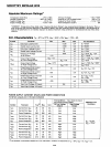
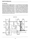
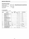
DEVICE SELECTION
-~
[I>
OS1
[g>
OS2
C'i:R
-
RESETS
DATA
LATCH
SETS
SR
FLlP·FLOP
(NO
EFFECT
ON
OUTPUT BUFFER)
STB
MD (DS,-
DS
2)
DATA
OUT EaUALS
~
0
0 0
3-STATE
,
0 0
3=STAte------
0
,
0
DATA
LATCH
,
,
0
DATA
LATCH
0
0
,
DATA
LATCH
~
0
1---
,
DATA IN
0
-,-
,
DATA
IN
,
, ,
DATA
IN
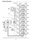
SERVICE REQUEST
FF
\
Service Request Flip-Flop
The
(SR)
flip-flop is used to generate and control
interrupts in microcomputer systems. It is asyn-
chronously set by the CLR input (active low). When
the
(SR)
flip-flop is.set
it
is in the non-interrupting
state.
The output of the
(SR)
flip-flop (Q) is connected to
an
inverting input
of
a
"NOR"
gate. The other input
to the
"NOR"
gate is non-inverting and is connected
to the device selection logic (081 • 082). The output
of the
"NOR"
gate (INT) is active low (interrupting
state) for connection to active low input priority
generating circuits.
STB (Strobe)
This input is used
as
the clock
(C)
to the data latch
for the
input
mode
MO
= 0) and to synchronously
reset the service request flip-flop (SR).
Note
that
the
SR
flip-flop
is
negative
edge
triggered.
5-102
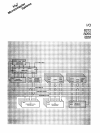
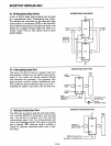
Output Buffer
The outputs of the data latch
(Q) are connected to
3-state,
non-inverting output buffers. These buffers
have a common control line (EN); this control line
either enables the buffer to transmit the data from
the outputs of the data latch
(Q) or disables the
buffer; forcing the output into a high impedance
state. (3 -state)
This high-impedance state allows the designer to
connect the
8212
directly onto the microprocessor
bi-directional data bus.
Control
Logic
The 8212 has control inputs 051, 052,
MO
and
STB. These inputs are used to control device selec-
tion, data latching, output buffer state and service
request flip-flop.
MD
(Mode)
This input is used to control the state of the output
buffer and to determine the source of the clock input
(C)
to the data latch.
When
MO
is high (output mode) the output buffers
are enabled and the source of clock
(C)
to the data
latch is from the device selection logic (051 •
OS2).
When
MD is low (input mode) the output buffer state
is
det~rmined
by the device selection logic
(OS1
•
OS2)
and the source of
clock
(C)
to the data latch is
the.STB (Strobe) input.
DS1, DS2
(Device
Select)
These 2 inputs are used for device selection. When
OS1
is low and
OS2
is high
(OS1
•
OS2)
the device is
selected.
In
the selected state the output buffer is
enabled and the service request flip-flop
(SR)
is
asynchronously set.
Functional Description
Data Latch
The 8 flip-flops that make up the data latch are of a
"0"
type design. The output (Q) of the flip-flop will
follow
th~
data input (0) while the clock input
(C)
is
high. Latching will occur when the clock
(C)
returns
low.
The data latch
is
cleared
by
an
asynchronous reset
input
(CLR). (Note: Clock
(C)
Overides
Reset
(CLR).)