SILICON GATE
MOS
8702A
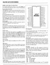
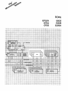
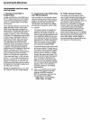
PIN CONNECTIONS
The
external
lead
connections
to
the
8702A
differ,
depending
on
whether
the
device
is
being
programmed
(1)
or
used
in
read.
mode. (See
following
table.)
12
13
14
15
16
22
23
MODE .
(Vee)
(Program)
(CS)·
(V
BB
)
(V
GG
)
(Vee)
(Vee)
Read
Vee
Vee
GND
Vee
V
GG
Vee
Vee
Programming
GND
Program Pulse
GND
Vee
Pulsed V
GG
(V,L4P )
GND
GND
ABSOLUTE MAXIMUM RATINGS·
Ambient
Temperature
Under
Bias
OOC
to
+
70
0
C
Storage
Temperature
-65°C
to
+125
0
C
Soldering
Temperature
of
Leads
(10
sec)
. . . . . .
..
+300
o
C
Power Dissipation 2 Watts
Read
Operation:
Input
Voltages and
Supply
Voltages
with
respect
to
Vee
+0.5V
to
-20V
Program
Operation:
Input
Voltages and
Supply
Voltages
with
respect
to
Vee
-48V
*COMMENT
Stresses above those
listed
under"
Absolute
Maximum
Rat-
ings"
may
cause
permanent
damage
to
the
device.
This
is a
stress
rating
only
and
functional
operation
of
the
device
at
these
or
at
any
other
condition
above those
indicated
in
the
operational
sections
of
this
specification
is
not
implied.
Exposure
to
Absolute
Maximum
Rating
conditions
for
ex-
tended
periods
may
affect
device rei
iabil
ity.
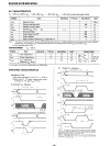
READ OPERATION
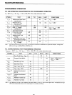
D.C. AND OPERATING CHARACTERISTICS
. (2) .
TA =
aoc
to
70
o
C,
Vee
=+5V±5%, V
oo
=
-9V±5%,
V
GG
=
-9V±5%,
unless otherwise noted.
SYMBOL
TEST
MIN.
TypJ3)
MAX.
UNIT
CONDITIONS
III
Address and Ch
ip
Select
10
fJA
V
IN
=
O.OV
Input
Load
Current
I
lO
Output
Leakage
Current
10
JJA
-
V
OUT
= O.OV,
CS
= V
ee
-2
1
000
Power
Supply
Current
5
10
mA
VGG=Vee,CS=Vee-2
10l
= O.OmA, TA =
2Soc
1
001
Power
Supply
Current
35
SO
mA
CS=V
cc
-2
""'"
10l
=O.OmA, T
A
= 2SoC
1
002
Power
Supply
Current
32
46
mA
CS=O.O
10l
=O.OmA, TA = 2SoC
>
Continuous
1
003
Power
Supply
Current
38.5
60
mA
CS=V
ec
-2
10l
=O.OmA , TA =
OOC
Operation
leF1
Output
Clamp
Current
8
14
mA
V
OUT
=
-l.QV,
T
A
=
OOC
leF2
Output
Clamp
Current
13
mA
V
OUT
=
-1.0V,
T
A
=2SoC
~
I
GG
Gate
Supply
Current
10
fJA
V
,l1
Input
Low
Voltage
for
-1.0
0.65
V
n L
Interface
V
1L2
Input
Low
Voltage
for
V
oo
Vec-
6
V
MOS
Interface
V
1H
Address and
Chip
Select
V
cc
-2
Vee +0.3
V
Input
High
Voltage
IOl
Output
Sink
Current
1.6
4
mA
V
OUT
=
0.45V
VOL
Output
Low
Voltage
-.7
0.45
V
IOl
=
1.6mA
V
OH
Output
High Voltage 3.5
V
IOH
=
-2001lA
Note
1:
In
the programming
mode,
the
data
inputs
1-8
are
pins
4-11
respectively.
es
=
GN
O.
Note
2:
VGG
may
be
clocked
to
reduce
power dissipation. In this
mode
average
100
increases
in
proportion
to
VGG
duty cycle.
(See
p.
5)
Note 3: Typical
values
are
at
nominal
voltages
and
TA = 25
0
C.
5-38


