


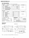

Silicon Gate MOS 8111-2
1024
BIT
(256
x
4)
STATIC MOS RAM
WITH COMMON
I/O
AND OUTPUT DISABLE
• Organization
256
Words by 4 Bits
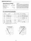
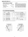
• Access Time -
850
nsec Max.
• Common Data Input and Output
• Single +
5V
Supply Voltage
• Directly TTL Compatible - All Inputs
and Output
• Static MOS - No Clocks
or
Refreshing Required
• Simple Memory Expansion - Chip
Enable Input
• Fully Decoded - On Chip Address
Decode
• Inputs Protected - All Inputs Have
Protection Against Static Charge
• Low Cost Packaging
-18
Pin Plastic
Dual-In-Line Configuration
• Low Power - Typically 150 mW
• Three-State Output - OR-Tie
Capability
The Intel®8111-2
is
a 256 word
by
4
bit
static random
access
memory element using
normally
off
N-channel
MOS devices integrated on a
monolithic
array.
It
uses
fully
DC
stable (static)
circuitry
and therefore requires
no clocks
or
refreshing
to
operate. The data
is
read
out
nondestructively and
has
the
same
polarity
as
the
input
data. Common
input/output
pins are provided.
The 8111-2
is
designed
for
memory applications in small systems where high performance,
low
cost, large
bit
storage, and simple interfacing are
important
design objectives.
It
is
directly
TTL
compatible in all respects: inputs, outputs, and a single
+5V
supply. Separate
chip
enable
(CEl leads
allow
easy
selection
of
an
individual package when
outputs
are OR-tied.
The Intel®8111-2
is
fabricated
with
N-channel silicon gate technology. This technology allows
the
design and
production
of
high performance, easy-to-use MOS circuits and provides a higher
functional
density on a mon-
olithic
chip than either conventional MOS technology
or
P-channel silicon gate technology.
Intel's silicon gate technology also provides excellent protection against contamination. This permits the
use
of
low cost silicone packaging.
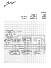
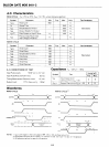
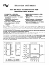
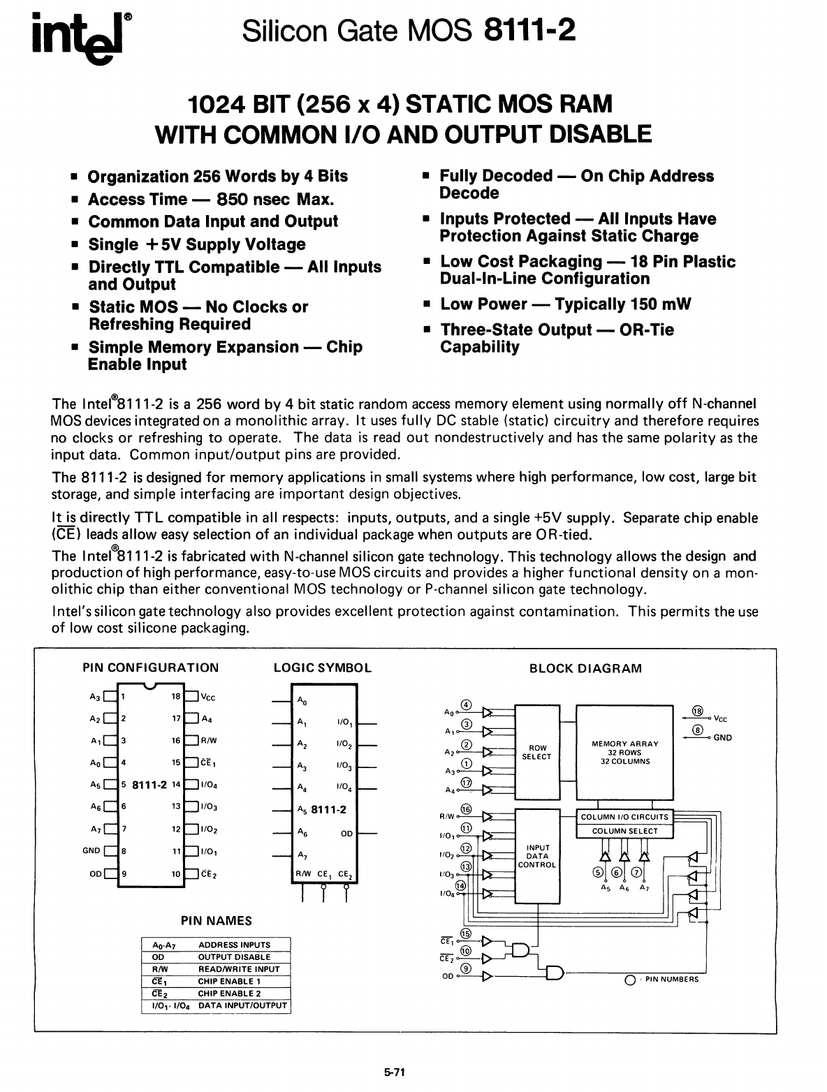
LOGIC
SYMBOL
BLOCK
DIAGRAM
o 'PIN NUMBERS
@
-------0
Vee
~GNO
MEMORY
ARRAY
32 ROWS
32
COLUMNS
ROW
SELECT
A
O
A,
I/O,
A
z
I/O
z
A
3
1/0
3
A
4
1/0
4
As 8111-2
AO-A7
ADDRESS INPUTS
00
OUTPUT DISABLE
RIW
READIWRITE INPUT
CE,
CHIP
ENABLE
1
CE2
CHIP
ENABLE
2
1/0,-
1/04
DATA
INPUT/OUTPUT
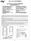
PIN
CONFIGURATION
A3
18
Vee
A2
17
A4
A,
16 R/W
Ao
4
15
tEl
As
5 8111-2 14
1/04
A6
6
13
1/03
A7
12
1/02
GNO
11
I/O,
00
9
10
CE2
PIN NAMES
5-71