


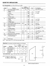
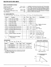
·SILICON GATE MOS 8080'A
- .
8080A
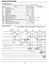
FUNCTIONAL
PIN
DEFINITION
The following describes
the
function
of
all
of
the
8080A
I/O pins.
Several
of
the
descriptions refer
to
internal timing periods.
_. .
A
1
5.
A
O (oU1put three-state)
ADDRESS BUS;.the address bus provides
the
address
to
memory
(up
to
64K 8-bit words)
or
denotes
the
I/O device
number
for up
to
256
input
and
256
output
devices.
Ao
is
the
least significant
address. bit.
OJ-D.o
(input/output
three-state)
DATA BUS;
the
data
bus provides bi-directional.communication
.between
the
CPU, memory, and
I/O.
devices
for
instructions and
data transfers. Also, during
the
first clock cycle
of
each machine
cycle,
the
8080A
outputs
a
status
word
on
the
data
bus
that
de.
_scribes
the
current
machine cycle. Do
is
the
least significant bit.
SYNC (output)
SYNCHRONlZING SIGNAL;
the
SYNC pin provides a signal
to
indicate
the
beginning-of each machine cycle.
DBIN (output)
DATA
BUS
IN;
the
DBIN signal indicates
to
external circuits
that
the
data
bus
is
in
the
input
mode. This signal should be used
to
enable
the
gating
of
data
onto
the
8080A
data
bus from memory
or
I/O.
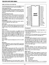
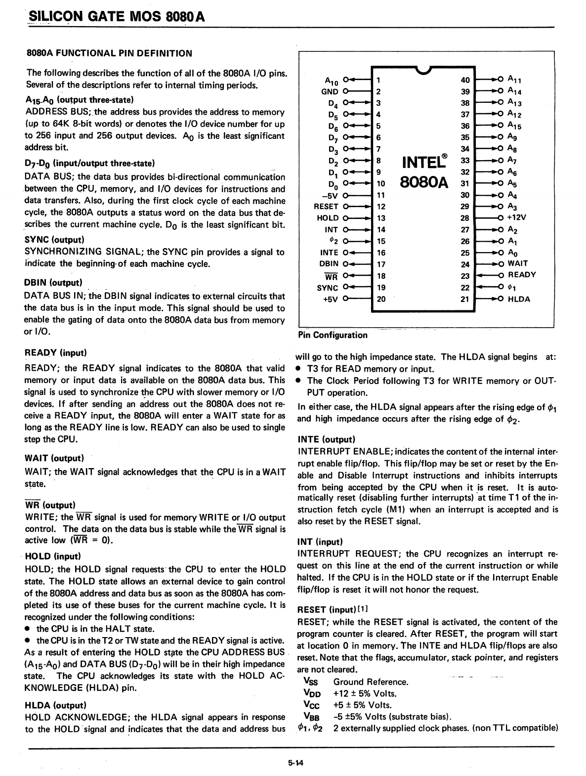
A
10
1
GNO 2
0
4
3
0
5
4
°6~5
0
7
6
0
3
7
O~
8
0
1
.0
9
DO
0 10
-5V
11
RESET 12
HOLD
13
INT
14
4>2
15
INTE 0 16
OBIN 0 17
WR
18
SYNC 19
+5V 20
-.
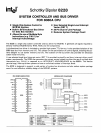
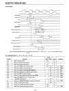
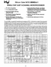
Pin
Configuration
INTE~
8080A
40
__
~'-JI
A
11
39 A
14
38 A
13
37 A
12
36 0 A
15
35 0 A
g
34 As
33 0 A
7
32
A
6
31
As
30 0 A
4
29 A
3
28 +12V
27
A
2
26 A
1
25 A
o
24 WAIT
23
READY
22
4>1
21
HLOA
REAPV
(input)
READY;
the
READY signal indicates
to
the
8080A
that
valid
memory
or
input
data
is
available
on
the
8080A
data
bus. This
signal
is
used
to
synchronize
t.he
CPU with slower memory
or
I/O
devices. If
after
sending an address
out
the
8080A
does
not
re-
ceive a READY input,
the
8080A
will
enter
a WAIT
state
for
as
long as
the
READY line
is
low. READY can also be used
to
single
step
the
CPU.
YlJAIT
(output)
WAIT;
the
WAIT signal acknowledges
that
th~
CPU
is
in
a WAIT
s~ate.
WR
(output)
WRITE;
the
WR
signal
is
used
for
memory WRITE
or
I/O
output
control.
The
data
on
the
data
bus
is
stable while
the
WR
signal
is
active low
(WR
= 0).
. HOLD (input)
HOLD;
the
HOLD signal requests'
the
CPU
to
'enter
the
HOLD
state.
The
HOLD
state
allows an external device
to
gain control
of
the
8080A
address and
data
bus as soon as
the
8080A
has com-
pleted its use
of
these buses for
the
current
machine cycle. It
is
recognized
under
the
following conditions:
•
the
CPU
is
in
the
HALT state.
•
the
CPU
is
in
the
T2
or
TW
stateand
the
READY signal
is
active.
As a result
of
entering
the
HOLD stf'te
the
CPU ADDRESS
BUS.
(A15-AO)
and DATA BUS
(0
7
-00)
will be
in
their
high impedance
state.
The
CPU acknowledges its
state
with
the
HOLD
AC-
KNOWLEDGE (HLDA) pin.
HLOA
(output)
HOLD ACKNOWLEDGE;
the
HLDA signal appears
in
response
to
the HOLD'signal and !ndicates
that
the
data
and address bus
will go
to
the
high impedance state.
The
HLOA signal begins at:
•
T3
for READ memory
or
input.
•
The
Clock Period following
T3
for
WR
ITE memory
or
OUT-
PUT operation.
In
either case,
the
HLOA signal appears
after
the
rising edge
of
4>1
and high impedance occurs
after
the
rising edge
of
4>2.
INTE (output)
INTER RUPT ENABLE; indicates
the
content
of
the
internal inter-
rupt
enable flip/flop. This flip/flop may be
set
or
reset by
the
En-
able. and Disable I
nterrupt
instructions and inhibits interrupts
from being accepted
by
the
CPU
when it
is
reset. It
is
auto-
, matically reset (dfsab'ling
further
interrupts) -at time
T1
of
the
in-
struction fetch cycle
(M
1)
when an
interrupt
is
accepted and
is
also reset
by
the
RESET signal.
INT
(input)
INTERR.UPT REQUEST;
the
CPU
recognizes an interrupt re-
quest
on
this line
at
the
end
of
the
current
instruction
or
while
halted. If
the
CPU
is
in
the
HOLD state
or
if
the
Interrupt
Enable
flip/flop
is
reset it will
not
honor
the
request.
RESET (input)
[1]
RESET; while
the
RESET signal
is
activated,
the
content
of
the
program
counter
is
cleared.
After
RESET,
the
program will
start
at
location 0
in
memory.
the
INTE and HLDA flip/flops are also
reset. Note
that
the
flags, accumulator, stack pointer, and registers
are
not
cleared.
Vss
Ground Reference.
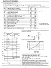
VDD
+12 ±
5%
Volts.
Vee
+5 ±
5%
Volts.
Vss
-5
±5%
Volts (substrate bias).
,l/>1,'l/>2
2 externally supplied clock phases. (non
TTL
compatible)
5-14