


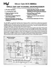
SILICON GATE MOS 8080A
A.C. CHARACTERISTICS (Continued)
TA =
O°C
to
70°C,
Voo
= +12V ±
5%,
Vee =
+5V
±
5%,
Vss
=
-5V'±
5%,
V
5
5 =
OV,
Unless Otherwise Noted
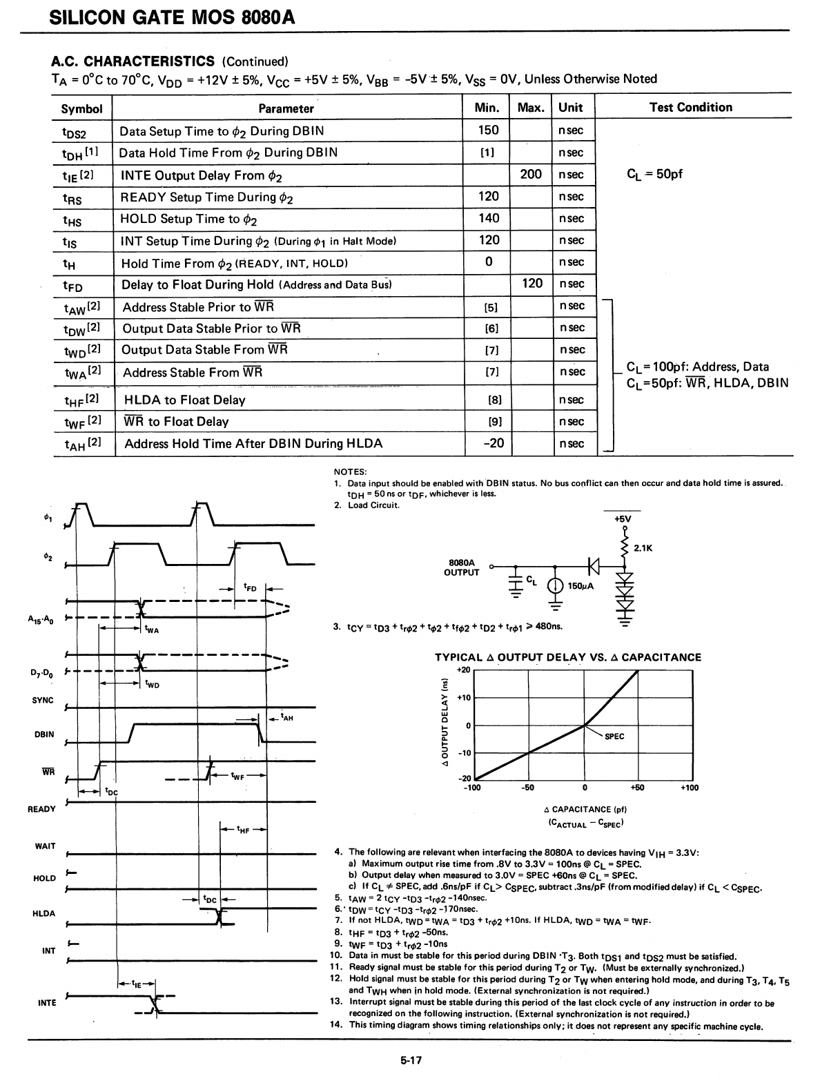
Symbol
Parameter
Min.
Max.
Unit
Test Condition
t052
Data Setup Time
to
~2
During
DBIN
150 nsec
tOH
(1)
Data Hold Time From
~2
During
DBIN
[1
]
nsec
tiE
[2)
INTE
Output
Delay From
~2
200
nsec
CL'=
50pf
tRS
READY
Setup Time During
~2
120 nsec
tH5
HOLD
Setup
Time
to
~2
140 nsec
tiS
I
NT
Setup Time During
~2
(During
cP1
in
Halt
Mode)
120
nsec
tH
Hold Time From
~2
(READY,
INT,
HOLD)
0 nsec
tFO
Delay
to
Float During Hold
(Address
and
Data
~us)
120
nsec
tAW
[2)
Address Stable Prior
to
WR
-
[5]
nsec
tow
[2)
Output
Data Stable Prior
to
WR
[6]
nsec
tWD[2]
Output
Data Stable From
WR
[7]
nsec
tWf\[2]
, Address Stable From
WR
[7]
nsec
~
CL= 100pf: Address, Data
.- -
C
L
=50pf:
WR,
HLDA,
DBIN
tHF[2]
HLDA
to
Float Delay
[8]
nsec
tWF[2]
WR
to
Float
Delay
[9]
nsec
tAH[2]
Address Hold
Time
After
DBIN
During
HLDA
-20
nsec
--
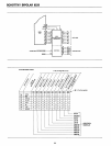
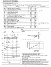
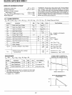
+5V
TYPICAL
~
OUTPUT
DELAY
VS. A
CAPACITANCE
+20
r-----~-----r----~---__.
+100
2.1K
+50
o
.:1.
CAPACITANCE
(pf)
(CACTUAL
- C
SPEC
)
-50
lit
..s
>
+10
«
..J
w
C
~
0
:;)
Q.
~
:;)
-10
0
<1
-20
-100
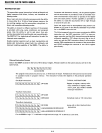
3.
tCY
=
t03
+
tr~2
+
t4>2
+
tf~2
+
t02
+ t
r
it>1
;>
480ns.
8080A
OUTPUT
NOTES:
1.
Data input should
be
enabled
with
'OBIN status. No bus
co~f1ict
can
then occur and data
hold
time
is
assured.
tOH =50
ns
or tOF, whichever
is
less.
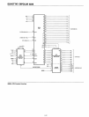
2.
Load Circuit.
4.
The
following
are relevant when interfacing
the
8080A
to
devices having
VIH
=
3.3V:
a)
Maximum
output
rise
time
from
.8V
to
3.3V
= 100ns@
CL
= SPEC.
b)
Output
delay when measured
to
3.0V
==
SPEC +60ns @
CL
==
SPEC.
c)
If
CL
"*
SPEC, add .6ns/pF
if
CL>
CSPEC, subtract .3ns/pF
(from
modified
delay)
if
CL
<
CSPEC.
5.
tAW
=2
tCY
-t03
-t
r
</>2
-140nsec.
6. •
tow
=tCY
-t03
-tr</>2
-l70nsec.
7.
If
not HLOA,
two
=tWA =
t03
+ t
r
</>2
+10ns.
If
HLOA,
two
=
twA
=
twF.
8.
tHF
==
t03
+t
r
c/>2
-50ns.
9.
twF
=
t03
+t
r
c/>2
-10ns
10. Data in must be stable
for
thisperiod
during
OBIN
·T3.
Both
tOS1 and tOS2 must be satisfied.'
11. Ready signal must be stable
for
thisperiod
during
T2
or
TW. (Must be
externally
synchronized.)
12. Hold signal must be stable
for
this period
during
T2
or
TW when entering
hold
mode, and during
T3,
T4,
TS
and TWH when in
hold
mode. (External synchronization
is
not
required.)
13.
Interrupt
signal must be stable duringthis period
of
the
last
clock
cycle
of
any instruction
in
order
to
be
recognized
on
the
following
instruction. (External synchronization
is
not
required.)
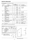
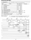
14. This
timing
diagram, shows
timing
relationships
only;
it
does
not
represent any specific machinecycle.
0
7
.0
0
~
SYNC
OBIN
WR
t
oc
READY
WAIT
HOLD
s-
t
oc
...-
HLDA
~
INT
I
-t:1-
INTE
5-17